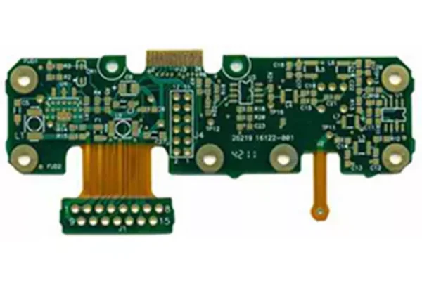
There is no such thing as a standard printed circuit board. Each board has a unique function for a particular product and must be designed to perform that function in the space allotted. Board designers use computer-aided design systems with special software to layout the circuit pattern on the board. A good PCB design can save PCB manufacturing price and prototyping time. Here are some very simple tips to better PCB design irrespective of the EDA tool used.
Table of Contents
1. Use hand-routing as much as possible.
CADs are not more intelligent than human mind. Unless it is very difficult, like multi-layer PCB with dozens of ICs, use hand-routing. It will be a much cleaner and neat design at the end.
2. Keep housing of final product in mind when designing layout.
Often we design PCB when no housing is decided. But at the end of the day they need to be housed. So keep mounting holes there, and better choose some readily available and simple housing and design around that. It is possible that later-on the same housing gets approved and the re-designing is avoided.
3. Use existing libraries as much as possible.
Why re-invent the wheel, it saves lots of time and helps to market product quickly. Search around and you will find libraries that suit for you.
4. When you design your component library, keep the pin layout as per datasheet.
Often the component pin-out arrangement is difference in schematic then the real physical layout. Try to design components according to the real layout. Why? Because when you place components around that component, say an IC, you can easily copy that arrangement in your PCB layout. His will help you to better components placement hence better PCB.
5. Arrange your designed library for good reference.
By this you will quickly located the parts and hence re-use the library for your future designs.
6. Arrange components on PCB as in your schematic.
What components are near, to say an MCU, keep them close in layout as well. Components like coupling capacitors need to be near the ICs, they are meant to be near. This will reduce the physical length of the traces on PCB. This will also help you to understand where different parts of a “system” are located and help while troubleshooting. In-fact placing components in the PCB layout is the key to PCB design. This is the “soul” of PCB design skill.
With the develop of new technology in electronics industry, the miniaturization of electronic products continues to drive printed circuit board manufacturing towards smaller and more densely packed boards with increased electronic capabilities. Advancements beyond the boards described here include three-dimensional molded plastic boards and the increased use of integrated circuit chips. These could be new challenges and opportunity for PCB designers.