THT plug-in process (through-hole insertion technology) and SMT process (surface mount technology) are two important processes in the field of electronic assembly. The following is their evolution process:
The Evolution of THT Plugin Technology
-Origin and Early Development: THT plugin process is an early electronic assembly technology, which can be traced back to the era of electronic tubes. In the early days, electronic products had simple structures and large component volumes. People manually inserted components with pins into the through holes of circuit boards and then soldered them to achieve electrical connections. At this time, the process mainly relies on manual operation, with low production efficiency and poor quality consistency.
-The stage of automation development: With the popularization and increasing demand for electronic products, manual plug-ins can no longer meet the requirements of large-scale production, so automatic plug-in machines have emerged. The automatic plug-in machine can quickly and accurately insert components into through holes, greatly improving production efficiency and plug-in accuracy. At the same time, the maturity of wave soldering technology has made the soldering process automated. By melting the tin waves on the circuit board, multiple solder joints can be soldered, further improving the production efficiency and quality stability of THT technology.
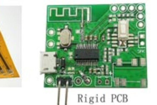
-Maturity and application expansion: The THT plugin process gradually matured in the mid-20th century and was widely used in various electronic products, such as early televisions, radios, computers, etc. Despite the rise of SMT technology later on, THT technology still plays a role in some specific fields, such as power electronics equipment and some modules in automotive electronics, due to its advantages in connecting high-power and high-voltage components, as well as its adaptability to the installation of some irregular components (such as large transformers, sockets, etc.).
The Evolution of SMT Technology
-The birth of technology: In the 1960s, SMT technology emerged to meet the demand for miniaturization of electronic products. The button shaped microdevices produced by Philips for watches have pioneered SMT technology. The United States was one of the earliest countries in the world to apply SMT, primarily in the fields of investment electronics and military equipment, utilizing its technological advantages to achieve miniaturization and high performance of products.
-Initial development: In the 1970s, Japan introduced SMT technology from the United States and applied it to the field of consumer electronics. Japan has invested heavily in strengthening the development and research of basic materials, basic technologies, and promotion applications, which has promoted the rapid development of SMT technology in the consumer electronics field. Products such as cameras and video recorders have begun to widely adopt SMT technology, greatly reducing their size and making their performance more stable.
-Rapid development: In the mid-1980s to early 1990s, SMT entered a stage of rapid development and gradually matured, becoming a new generation of circuit assembly technology. With the development of ultra large scale integrated circuits, the size of components continues to decrease, and the advantages of SMT technology are becoming increasingly apparent. It can achieve higher assembly density, meet the growing functional integration needs of electronic products, and gradually replace THT technology as the mainstream technology for electronic assembly.
-Modernization stage: Since the 1990s, SMT technology has continuously developed towards micro assembly, high-density assembly, and three-dimensional assembly technology. With the rise of portable electronic products such as smartphones and tablets, higher requirements have been put forward for SMT technology, such as the ability to handle smaller components (such as 0201, 01005 and other micro components), and achieve higher precision mounting and soldering. At the same time, the development of technologies such as 3D packaging and multi chip modules has further expanded the application scope and technical depth of SMT technology.
Get your exclusive quote immediately: fill out the form or send an email directly.As a professional PCB manufacturer for hobbyist , we will provide you with a quote service within 24 hours. Enjoy free DFM optimization and a 10% discount on SMT patches for your first order!