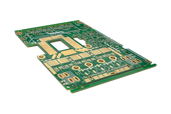
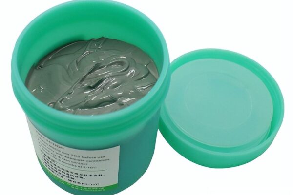
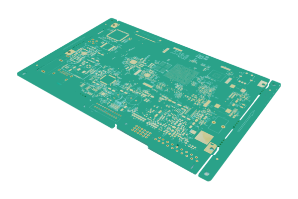
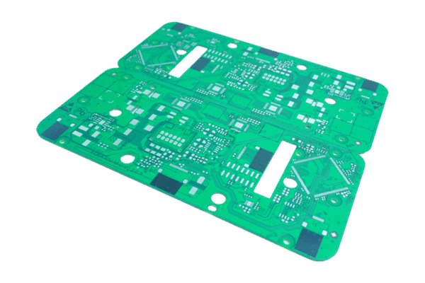
Printed Circuit Board Assembly (PCBA) files are critical for ensuring a smooth and efficient manufacturing process. These files provide essential information for component placement, soldering, and testing. However, errors in PCBA files can lead to production delays, increased costs, and defective products. This article highlights some of the most common mistakes in PCBA files and how to avoid them.
Table of Contents
1. Incomplete or Incorrect Bill of Materials (BOM)

The Bill of Materials (BOM) is a fundamental document in PCBA manufacturing, listing all required components. Common mistakes include:
Missing components or incorrect part numbers.
Inconsistent reference designators between the BOM and PCB design files.
Incorrect supplier information, leading to sourcing issues.
Lack of alternative part numbers for components with supply constraints.
Solution
To prevent these issues, always cross-check the BOM with the PCB design and ensure it aligns with component availability from suppliers.
2. Misaligned or Missing Component Footprints
Errors in component footprints can cause significant manufacturing issues, such as misaligned solder pads, incorrect pad sizes, or missing footprints. These issues often result in poor soldering, open circuits, or short circuits.
Solution
Validate footprints using design rule checks (DRC) in PCB design software and compare them with component datasheets before finalizing the design.
3. Incorrect Gerber Files or Missing Layers
Gerber files define the PCB layout for manufacturing. Mistakes in these files can lead to fabrication errors, including missing traces, incorrect layer assignments, or reversed polarity in silk screen layers.
Solution
Always generate and review Gerber files thoroughly using a Gerber viewer before submission. Ensure all necessary layers, including copper, solder mask, and silkscreen, are present and correctly aligned.
4. Insufficient Solder Mask Clearance
Solder mask clearance issues, such as overlapping solder mask on pads, can lead to unintended solder bridges or poor soldering quality.
Solution
Follow standard solder mask clearance guidelines and conduct a detailed design review to detect potential mask-related defects.
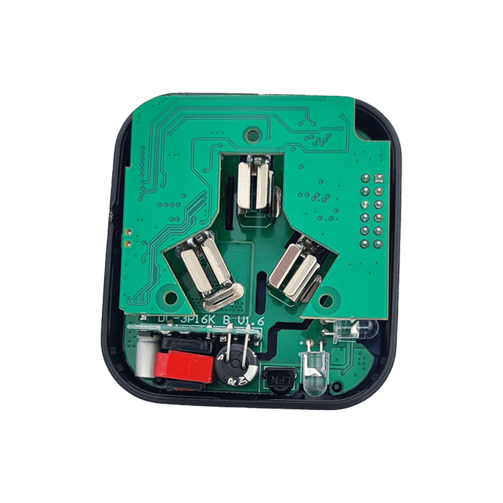
5. Inconsistent Component Polarity Markings
Incorrect or missing polarity markings for polarized components (such as diodes and electrolytic capacitors) can lead to improper assembly and functional failures.
Solution
Ensure clear polarity markings on the silkscreen and verify them against the BOM and assembly drawings.
6. Overlapping Designators and Silk Screen Issues
Overlapping reference designators, especially on dense PCB layouts, can lead to confusion during assembly, making manual inspection and rework difficult.
Solution
Position designators clearly and avoid placing them on component pads or critical areas. Use automated design verification tools to check silkscreen clarity.
7. Lack of Assembly and Test Points
Missing test points or improper test pad placement can make in-circuit testing (ICT) and functional testing difficult, reducing the ability to identify and fix manufacturing defects.
Solution
Design PCBs with adequate test points for key signals and ensure accessibility for testing probes and fixtures.
8. Incorrect Pick-and-Place (Centroid) Files
Pick-and-place files guide automated machines for component placement. Common mistakes include:
Incorrect X/Y coordinates.
Missing or misaligned rotation angles.
Inconsistent reference designators with the BOM and PCB layout.
Solution
Review pick-and-place files in manufacturing software to verify component positions and orientations before production.
Conclusion
Avoiding common mistakes in PCBA files is essential for ensuring efficient and error-free production. By thoroughly reviewing BOMs, Gerber files, footprints, solder mask clearances, and test point placements, manufacturers can minimize errors and enhance product quality. Implementing robust design verification and manufacturing checks will lead to smoother production processes and reduced costs in PCBA manufacturing.
Get your exclusive quote immediately: fill out the form or send an email directly.As a professional PCB manufacturer for hobbyist , we will provide you with a quote service within 24 hours. Enjoy free DFM optimization and a 10% discount on SMT patches for your first order!


