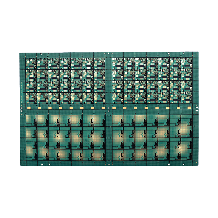
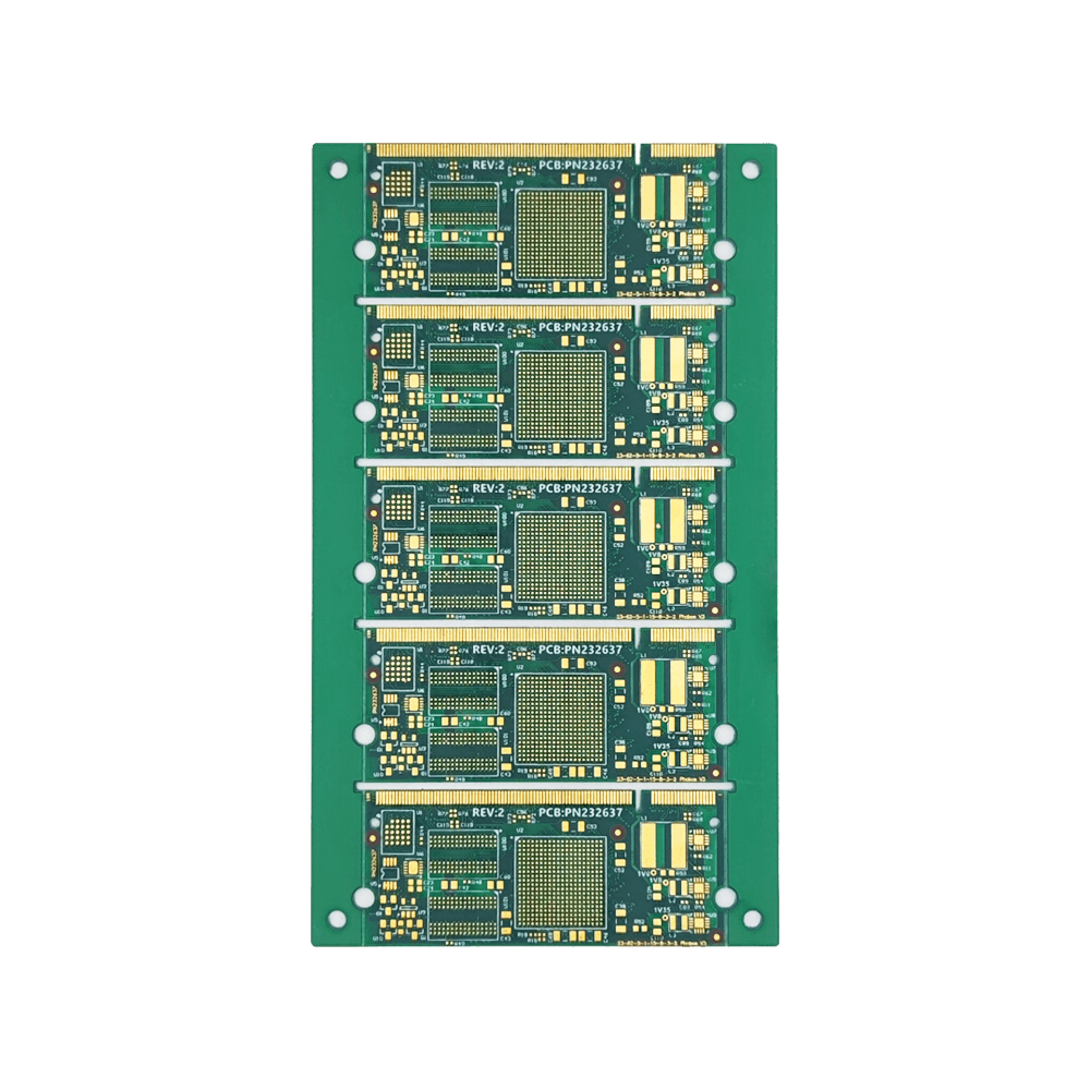
PCB Panelization refers to combining multiple identical or different PCB designs on a large substrate for mass production, improving production efficiency, and reducing costs. Here are some common rules and precautions for PCB layout:
Table of Contents
Ⅰ.Basic rules of layout design
1. Selection of layout method
-Same layout: Arrange multiple identical PCBs in rows and columns, suitable for mass production of a single product.
-Mixed layout: When combining different types of PCBs in the same layout, attention should be paid to whether the process requirements (such as solder pads and solder mask layers) of each PCB are compatible.
-Template shape: Try to keep the overall template rectangular or square to avoid irregular shapes and reduce material waste.
2. Size restrictions for imposition
-It needs to meet the maximum processing size of PCB production equipment (such as the worktable of printing machines and surface mount machines), with a common maximum size of 300mm × 400mm.
-At least 5mm of process edge should be reserved at the edge of the layout for installing positioning holes, Mark points (optical positioning points), and equipment clamping.
3. Positioning and Marking
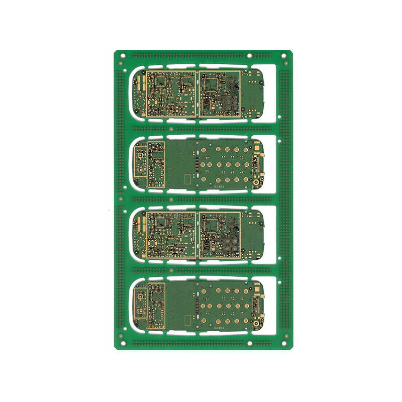
-Mark points: Each panel should have at least 3 Mark points (triangular distribution) placed for optical positioning during SMT surface mounting. The diameter is usually 1mm, and the surface should be flat, without solder pads or solder mask layers.
-Positioning hole: Set a circular hole with a diameter of 1.5-3mm on the process edge for mechanical positioning of PCB on the production line.
-Identification information: The product model, version number, production date, and assembly quantity should be marked on the assembly for easy traceability.
Ⅱ.Splicing Connection and Splitting Rules
1. Splicing connection method
-V-Cut: Cutting V-shaped grooves between PCB boards, suitable for substrates with a thickness ≤ 1.6mm. It can be manually broken or separated with a slitting machine during board splitting. The V-Cut depth is usually 1/3-1/2 of the plate thickness, and the groove width is 0.2-0.3mm.
-Stamp Slot Hole: Connected to PCB through a row of small holes (diameter 0.5-1mm), suitable for irregular shapes or thin boards, with neat edges after board separation.
-Routing: Milling grooves with a width of 0.8-1.2mm between PCBs, suitable for thick plates or scenarios requiring high-precision board splitting, which requires cutting with a milling cutter.
2. Requirements for board spacing
-V-Cut spacing: A spacing of ≥ 0.3mm should be reserved between adjacent PCBs to ensure that the solder pads or circuits are not damaged during board splitting.
-Stamp hole spacing: The distance between holes is ≤ 0.5mm, and the distance between hole edges and PCB edges is ≥ 0.5mm.
-Milling groove spacing: groove width ≥ 0.8mm, groove edge distance from components on PCB ≥ 1.5mm, to avoid damaging components during board splitting.
3. Board direction and stress control
-The direction of board splitting should be consistent with the fiber direction of the PCB (the pattern during board pressing) to reduce stress deformation during board splitting.
-For the separation area near sensitive components such as BGA and QFP, it is necessary to increase the protection spacing (≥ 2mm) or use milling grooves instead of V-Cut to reduce the impact of separation stress on the components.
Ⅲ.Compatibility rules for processes and production
1. Design of solder pads and solder mask layers
-The PCB at the edge of the layout must ensure the integrity of the solder pads to avoid cutting them due to the layout connection structure (such as V-Cut).
-The solder mask layer should cover the splicing connection area to prevent solder from overflowing onto adjacent PCBs during soldering.
2. Component layout and layout direction

-The component layout of each PCB in the layout should be consistent to avoid frequent parameter adjustments of the placement machine due to different directions.
-For components with polarity or direction requirements (such as ICs and capacitors), the direction should be unified in the layout to reduce surface mount errors.
3. Quantity of imposition and production efficiency
-The number of panels needs to balance production efficiency and cost: too many panels may result in oversized panels, affecting equipment processing; If the quantity is too small, the material utilization rate will be low. The common splicing quantity is 4-16 pieces.
-For small-sized PCBs (such as ≤ 50mm × 50mm), a “layout+sub layout” structure can be used (such as 2 × 2 large layouts, each containing 4 × 4 small PCBs) to improve production efficiency.
Ⅳ.Spelling rules for special scenarios
1. Flex Rigid PCB
-The splicing of flexible and rigid areas should avoid setting V-Cut or stamp holes in the flexible area, and adopt milling groove separation to prevent flexible circuit breakage.
-Sufficient margin (≥ 2mm) should be reserved in the flexible zone to avoid damage to the circuit caused by pulling during board splitting.
2. High frequency/high-speed PCB
-When assembling, it is necessary to ensure the integrity of the grounding and signal layers of each PCB to avoid electromagnetic interference (EMI) caused by the assembly connection structure.
-For circuits with high impedance control requirements, an overall impedance test must be conducted after layout to ensure that partitioning does not affect signal transmission.
3. Heat dissipation and thermal management
-For PCBs with high density of high-power components, the heat dissipation path should be considered during layout to avoid local high temperatures caused by over dense layout.
-When assembling metal substrates (such as aluminum substrates), attention should be paid to the depth of milling grooves to prevent damage to the heat dissipation layer during cutting.
Ⅴ.Key points for checking layout design
-DFM (Design for Manufacturing) inspection: Use PCB design software (such as Altium Designer, Eagle) DFM tools to verify whether the layout size, board spacing, Mark point position, etc. meet production requirements.
-Board splitting simulation: Simulate the board splitting process through software to check for stress concentration areas or component interference issues.
-Communicate with PCB manufacturers: Confirm the layout rules with the manufacturer in advance, as there may be slight differences in equipment and processes from different manufacturers (such as V-Cut minimum spacing and Mark point accuracy requirements).
Summarize
The core of PCB Panelization is to optimize production efficiency and cost while ensuring product quality. When designing, it is necessary to comprehensively consider factors such as board partitioning, size limitations, and process compatibility, and continuously optimize the solution through DFM tools and feedback from manufacturers. Reasonable layout design can reduce waste, improve surface mount efficiency, and reduce the risk of component damage during the board splitting process.
Get your exclusive quote immediately: fill out the form or send an email directly.As a professional PCB manufacturer for hobbyist , we will provide you with a quote service within 24 hours. Enjoy free DFM optimization and a 10% discount on SMT patches for your first order!