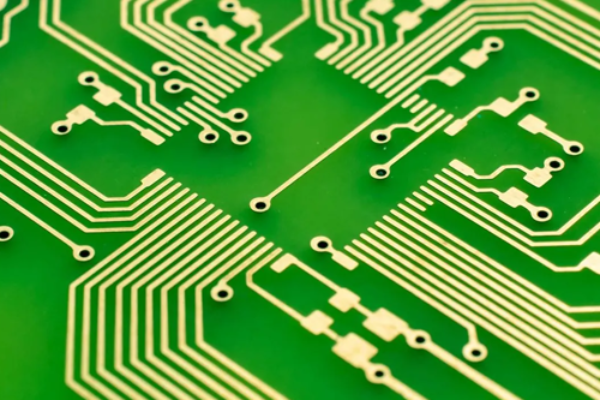
Factors affecting PCB soldering quality
From PCB design to the soldering of all components into a high-quality circuit board, it requires strict control of PCB design engineers, soldering processes, and the level of soldering workers.
There are mainly the following factors that will affect the quality of PCB soldering: PCB drawing, quality of circuit boards, quality of components, degree of oxidation of component pins, quality of solder paste, printing quality of solder paste, accuracy of placement machine programming, the placement quality of the placement machine, the setting of the temperature curve of the reflow oven, etc.
Among them, PCB drawing is an insurmountable link. Because people who do circuit design often do not solder circuit boards, they cannot gain direct soldering experience and do not know the various factors that affect soldering; while soldering workers do not understand drawing boards, they just complete the production tasks, and have no thought or ability to analyze the resulting causes of bad soldering. Since the two talents perform their respective duties, it is difficult to combine them organically.
Advice when drawing PCB diagrams
Next, I will give some suggestions to engineers on the process of PCB drawing, hoping to avoid various bad drawing methods that affect the soldering quality during the drawing process.
About tooling hole
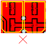
Four holes (minimum diameter of 2.5mm) should be left at the four corners of the PCB board for positioning the circuit board when printing solder paste. The center of the circle in the X-axis or Y-axis direction is required to be on the same axis, as shown in the following figure:
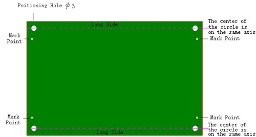
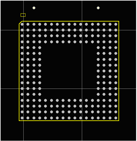
About the mark point
Used for placement machine positioning. Mark points should be marked on the PCB board, and the specific location: on the diagonal corner of the board, it can be a circular or square pad, and do not mix it with the pads of other components. If there are components on both sides, both sides should be marked.
Please note the following:
a. The shape of the Mark point is as follows. (up and down symmetry or left and right symmetry)

b. The size of A is 2.0mm.
c. Within the range of 2.0mm from the outer edge of the Mark point, there should be no shape and color changes that may cause wrong identification. (pad, solder paste etc.)
d. The color of the mark point should have a light and dark difference with the color of the surrounding PCB.
e. In order to ensure the recognition accuracy, the surface of the mark point is electroplated with copper or tin to prevent surface reflection. For markings whose shapes are only lines, optical points cannot be recognized.
As shown below:
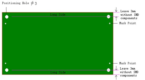
About leaving 5mm edge
When drawing the PCB, leave no less than 3mm in the long side direction for the placement machine to transport the circuit board. The placement machine cannot mount devices within this range. Do not place SMD devices within this range.
As shown below:
For circuit boards with components on both sides, should be considered that during the second reflow, it will rub off the components that have been soldered near the edge of the board, and in severe cases, the pads will be rubbed off and the circuit board will be damaged. As shown below:
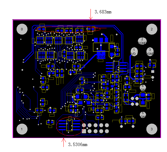
Therefore, it is recommended that the long side with fewer components (usually the bottom side) should not be placed components within 5mm of the edge of the board. If it is indeed due to the limited area of the circuit board, you can add Break away tab on the long side.
Do not place vias directly on the pads
The defect of the via hole directly on the pad is that the solder paste melts and flows into the via hole during reflow, resulting in a lack of tin on the device pad, thereby forming a virtual soldering. As shown in the figure:
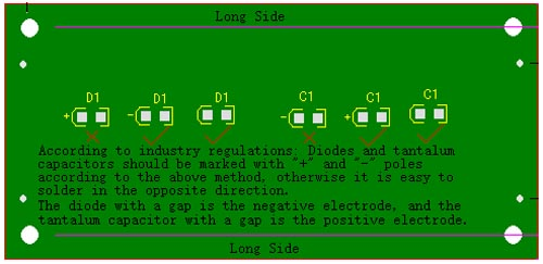
Polarity marking of diodes and tantalum capacitors
The polarity marking of diodes and tantalum capacitors should be in accordance with the industry regulations, so as to prevent workers from soldering in the wrong direction based on experience. As shown in the figure:
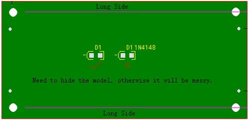
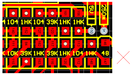
About silkscreen and mark
Please hide the part number. Especially circuit boards with high device density, otherwise, dazzling affects finding the soldering position. As shown below:
Don’t just mark the description, not the designator. As shown in the figure below, the placement machine cannot be programmed.
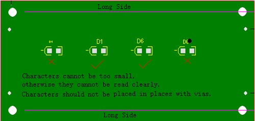
The size of the silkscreen characters should not be so small that they cannot be seen clearly. The placement of characters should be staggered hole to avoid misreading.
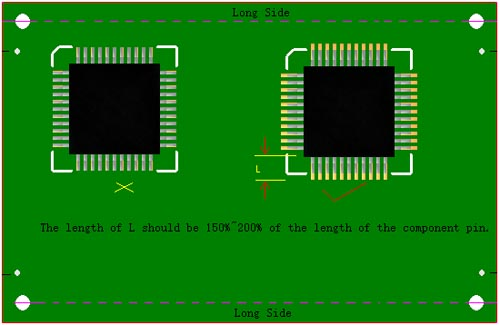
About IC pads should be extended
SOP, PLCC, QFP and other packaged ICs should extend the pad when drawing the PCB. The length of the pad on the PCB = the length of the IC foot × 1.5 is suitable, so that it is convenient for manual soldering with a soldering iron. IC foot, PCB pad and tin melt into one. As shown in the figure:
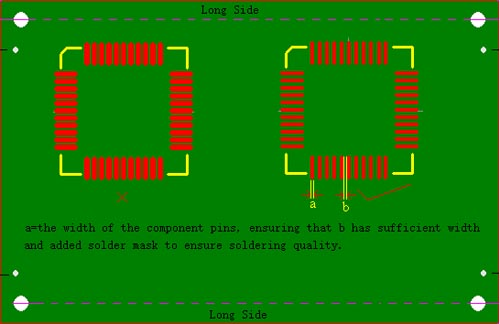
About the width of IC pads
SOP, PLCC, QFP and other packaged ICs, pay attention to the width of the pad when drawing the PCB. The “a” width of the pad a on the PCB = the width of the IC foot (ie: Nom. value in the datasheet), please do not widen it, and ensure that “b” (ie between the two pads) have enough width to avoid tin connection. As shown in the figure:
Place the components not to rotate at arbitrarily angle
Since the placement machine cannot rotate at arbitrarily angle, it can only rotate at 90°C, 180°C, 270°C, and 360°C. As shown in Figure B below, if it is rotated by 1°C, after the placement machine is mounted, the components pins and the pads on the circuit board will be staggered by an angle of 1°C, which will affect the soldering quality.
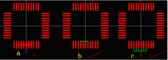
Matters needing attention when short-circuiting adjacent pins
The short-circuiting method in Figure a below is not conducive for workers to identify whether the pin should be connected, and it is not beautiful after soldering. If you short-circuit and add solder mask according to the method of Figure b and Figure c when drawing, the effect of soldering will be different: as long as each pin is not connected, the chip will not be short-circuited, and the appearance will be beautiful.
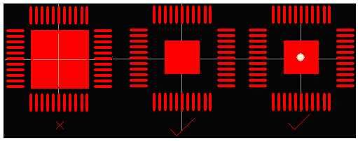
Question about the middle pad under the chip
When drawing a chip with a pad in the middle under the chip, if according to the package diagram of the chip to draw the middle pad, it is easy to cause a short circuit. It is recommended to shrink the pad in the middle so that it has a greater distance from the surrounding pin pads, thereby reducing the chance of a short circuit. As shown below:
Two components with a higher thickness should not be placed close together
As shown in the figure below, this layout will cause the placement machine to touch the previously placed component when placing the second component and the machine will detect the danger and cause the machine to automatically power off.
About BGA
Because the BGA package is special, its pads are all under the chip, and the soldering effect cannot be seen outside. For the convenience of repairing, it is recommended to layout two positioning holes of Hole Size: 30mil on the PCB board, so that the stencil can be positioned during repairing.
Reminder: The size of the positioning hole should not be too large or too small. It is advisable to make the needle not fall off, not shake after insertion, and a little tight when inserted, otherwise the positioning will not be accurate. As shown below:
Moreover, it is recommended that a certain area around the BGA should be set aside for placing devices, so that the stencil can be placed during rework.
About PCB board color
It is recommended not to make red. Because the red circuit board is white under the red light source of the camera of the placement machine, it cannot be programmed, and it is not convenient for the placement machine to solder.
About small components below large components
Some people like to arrange the small components under the large components on the same layer, for example: there is a resistor under the digital tube, as shown below:
Such design will cause difficulties in repairing, and the digital tube must be dismantled before repairing, which may also cause damage to the digital tube. It is recommended to arrange the resistor under the digital tube to the another side, as shown below:
About the connection between copper and the pad to affect the melting of tin
Since the copper coating will absorb a lot of heat, it is difficult for the solder to fully melt, resulting in a virtual soldering. As the picture shows:

In Figure a, the component pads are directly connected to the copper cladding; in Figure b, the 50Pins connector is although not directly connected to the copper cladding, but since the middle two layers of the four-layer board are large-area copper cladding, both Figures a and b will be covered by the copper cladding. Copper absorbs a lot of heat and the solder paste does not melt sufficiently. The body of the 50Pins connector in Figure b is a plastic that is not resistant to high temperature. If the temperature is set high, the body of the connector will melt or deform. If the temperature is set low, the copper coating absorbs a lot of heat and the solder paste cannot be fully melted. Therefore, it is recommended that the pads be isolated from the large area copper. As the picture shows:
Suggestions on panel and Break away tab
Summarize
Nowadays, there are more and more engineers who can use software to draw, wire and design PCBs, but once the design is completed, and can greatly improve the soldering efficiency, the author believes that it is necessary to pay attention to the above elements. And to develop good drawing habits, to be able to communicate well with the processing factory, is what every engineer must consider.
Hot tags: drawing PCB diagrams, circuit board drawing, PCB soldering, pcb stencil, smt stencil, circuit board soldering near me, pcb soldering service, stencil in pcb, through hole soldering board, components, Customized, cheap, quotation, suppliers, factory, manufacturer, manufacturing, manufacturing services