Whether it’s during the initial setup, or due to human error, connecting power supply terminals in reverse can lead to short circuits, component failure, and system malfunctions. An effective anti-reverse connection circuit design ensures that devices remain operational even when the input power is incorrectly connected.
Table of Contents
The Importance of Anti-reverse Protection
When an electrical device is connected to a power source, the correct polarity must be ensured to avoid damaging components such as diodes, transistors, integrated circuits (ICs), and other semiconductor elements. A reverse connection can cause:
Overheating: Components may overheat due to excessive current flow.
Component Failure: Some components, like electrolytic capacitors and diodes, may fail instantly when exposed to reverse voltages.
Power Supply Damage: The power supply itself might burn out or enter a failure mode if it lacks protection.
Thus, incorporating anti-reverse protection into the power supply circuit is not only a safety measure but also a way to enhance the reliability of the entire system.
Generally, the following methods are commonly used:
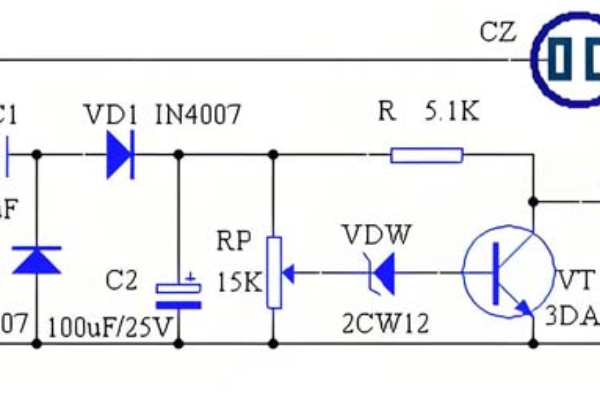
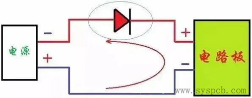
1. Diode series anti-reverse connection protection circuit
A forward diode is connected in series at the input terminal of the positive power supply to make full use of the characteristics of the forward conduction and reverse cutoff of the diode. Normally, the diode conducts and the board works.
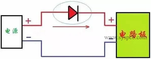
When the power supply is reversed, the diode is cut off, the power supply cannot form a loop, and the circuit board does not work, which can effectively prevent the problem of reversed power supply. But there will be a diode voltage drop, and it is also important to choose the corresponding diode according to the supply current.
2. Rectifier bridge type anti-reverse connection protection circuit
Use a rectifier bridge to change the power input into a non-polar input, no matter whether the power is connected positively or reversely, the circuit board will work normally.
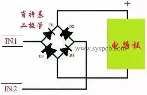
The above uses diodes for anti-reverse treatment. If silicon diodes are used, the voltage drop will be about 0.6, 0.8V, and germanium diodes will also have a voltage drop of about 0.2, 0.4V. If the voltage drop is too large, you can use MOS tubes for anti-reverse treatment. The voltage drop of the MOS tube is very small, up to a few milliohms, and the voltage drop is almost negligible.
3. MOS tube anti-reverse protection circuit
Because of factors such as the improvement of the MOS tube process and its own properties. Most of its conduction internal resistance is milliohm level or even smaller, so the loss caused by the voltage drop and power consumption of the circuit is very small, or even negligible, so it is recommended to choose a MOS tube to protect the circuit Way.
(1) NMOS protection
As shown in the figure below: at the moment of power-on, the parasitic diode of the MOS tube is turned on, and the system forms a loop. The potential of the source S is about 0.6V, and the potential of the gate G is VBAT, and the turn-on voltage of the MOS tube is extremely: UGS = VBAT – Vs, the gate shows a high level, the DS of the NMOS is turned on, the parasitic diode is short-circuited, and the system forms a loop through the DS of the NMOS.
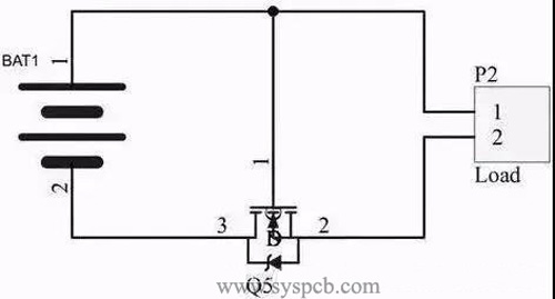
If the power supply is reversed, the conduction voltage of the NMOS is 0, the NMOS is cut off, the parasitic diode is reversed, and the circuit is disconnected, thereby forming a protection.
(2) PMOS protection
As shown in the figure below: at the moment of power-on, the parasitic diode of the MOS tube is turned on, and the system forms a loop. The potential of the source S is about Vbat-0.6V, while the potential of the gate G is 0, and the turn-on voltage of the MOS tube is extremely: UGS = 0 -(Vbat-0.6), the gate is low level, the DS of the PMOS is turned on, the parasitic diode is short-circuited, and the system forms a loop through the DS of the PMOS.

If the power supply is reversed, the conduction voltage of the NMOS is greater than 0, the PMOS is cut off, the parasitic diode is reversed, and the circuit is disconnected, thereby forming a protection.
If the power supply is reversed, the conduction voltage of the NMOS is greater than 0, the PMOS is cut off, the parasitic diode is reversed, and the circuit is disconnected, thereby forming a protection.
Note: The NMOS transistor connects DS to the negative pole, the PMOS transistor DS connects to the positive pole, and the direction of the parasitic diode faces the current direction of the correct connection.
The connection of the D pole and the S pole of the MOS tube: when using an N-channel MOS tube, the current generally enters from the D pole and flows out from the S pole, while the PMOS enters from the S pole and flows out from the D pole. In the circuit, it is just the opposite, and the voltage condition for the MOS transistor to be turned on is met through the conduction of the parasitic diode. As long as an appropriate voltage is established between the G and S poles, the MOS tube will be fully turned on. After it is turned on, it is like a switch is closed between D and S, and the current is the same resistance from D to S or S to D.
In practical applications, the G pole is generally connected in series with a resistor. In order to prevent the MOS tube from being broken down, a Zener diode can also be added. The capacitor connected in parallel to the voltage divider resistor has a soft start effect. At the moment when the current starts to flow, the capacitor is charged, and the voltage of the G electrode is gradually established.
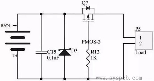
For PMOS, compared with NOMS, VGS is required to be greater than the threshold voltage. Since its turn-on voltage can be 0, the voltage difference between DS is not large, which is more advantageous than NMOS.
4. Fuse protection
For many common electronic products, after disassembly, you can see that the power supply has a fuse. When the power supply is reversed and there is a short circuit in the circuit, the fuse will be blown due to a large current to protect the circuit. However, this method it is more troublesome to repair and replace. But you can choose to buy resettable fuses.
Choosing the Right Anti-reverse Protection
When designing anti-reverse connection circuits, several factors need to be considered:
Current Handling Capacity: Ensure the protection components can handle the maximum expected current without failure.
Voltage Rating: Components should be rated for the maximum input voltage to prevent breakdown or failure.
Efficiency: For battery-powered or energy-efficient systems, minimizing power loss due to voltage drops (from diodes or relays) is critical.
Cost and Complexity: The design should balance simplicity, cost, and protection needs.
For simple applications, a diode-based protection circuit might suffice, while more complex systems might require MOSFETs or polarity protection ICs for higher efficiency and additional protection features.
Conclusion
Power supply anti-reverse connection protection is a critical consideration in the design of any electronic device that relies on external power sources. By implementing the right protection mechanisms—whether through diodes, relays, MOSFETs, or specialized ICs—designers can ensure the long-term reliability and safety of their products. With the variety of available protection methods, it’s essential to choose the one that best matches the specific needs of the application, balancing cost, complexity, and performance.
Hot tags: circuit design, pcb design, custom pcb, pcb online, pcb maker, circuit simulator, pcb board design, pcb design online, circuit board design, electronic circuit simulator, Customized, cheap, quotation, suppliers, factory, manufacturer, manufacturing, manufacturing services