Precision PCB Fabrication, PCB Assembly, DIP Assembly, BGA Assembly etc..
We provide the most competitive PCB & PCBA services.
- All
- Product Name
- Product Keyword
- Product Model
- Product Summary
- Product Description
- Multi Field Search


The inductor has alternating current, and the copper on the bottom of the inductor will generate eddy current on the ground plane. The eddy current effect will affect the inductance of the power inductor, and the eddy current will also increase the loss of the system. At the same time, the noise generated by the alternating current will increase the noise on the ground plane,will affect the stability of other signals.
From the EMC point of view, laying copper on the bottom of the inductor, and laying copper on the complete ground plane is beneficial to the design of EMI; the current production process of inductors is upgraded, and the inductors use shielded inductors, and there are few magnetic induction lines that leak, and the inductance of the inductors is very small. The amount has little effect, and it can also help to dissipate heat.
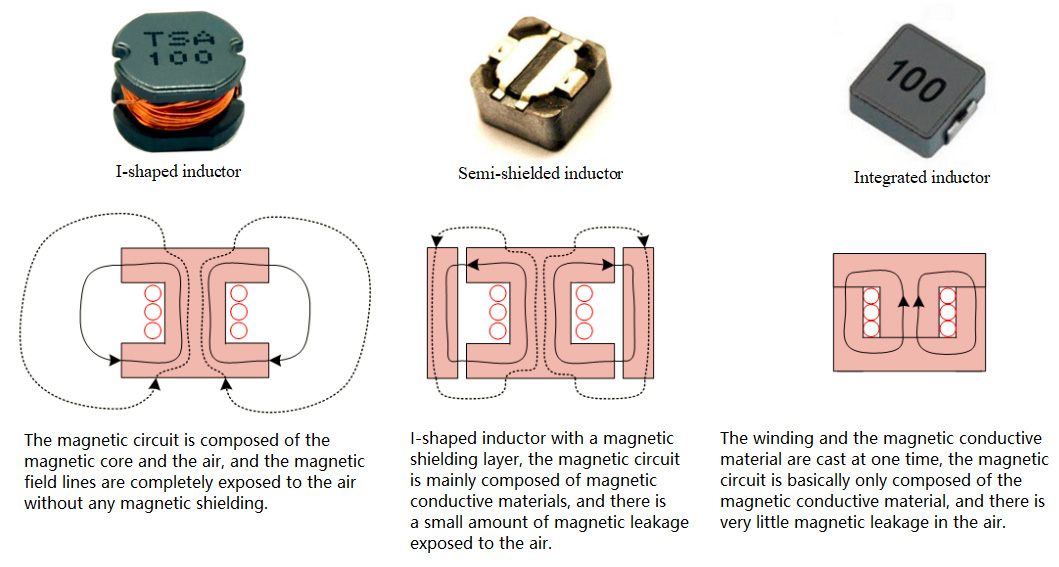
How to choose in the project, we must first understand the structure of the inductor. Our commonly used inductors include unshielded I-shaped inductors, semi-shielded inductors, and integrated inductors. So what are their characteristics?
The winding and the magnetic conductive material are cast at one time, the magnetic circuit is basically only composed of the magnetic conductive material, and there is very little magnetic leakage in the air
The unshielded I-shaped inductor, the magnetic circuit is composed of the magnetic core and the air, and the magnetic field lines are completely exposed to the air without any magnetic shielding.
The semi-shielded inductor can be seen from its skeleton structure. On the basis of the I-shaped inductor, a magnetic shielding material is added to the periphery of the inductor. Because the magnetic resistance of the magnetic shielding material is small, the magnetic field lines are basically locked in the magnetic conductive material, and only a small part of the magnetic field will leak out from the air gap, so it can play a certain shielding role.
The integrated inductor is made by casting the winding and the magnetic conductive material at one time during the production of the inductor. There is only a small air gap inside to prevent the inductor from saturating, so this inductor basically has no magnetic field line overflow.
In the experiment, we use a certain buck chip evaluation board of MPS to conduct an experiment. To simulate placing a copper layer under the inductor, we place a grounded copper pad near the inductor and measure the inductor current ripple to evaluate the effect of placing copper under the inductor.
Experimental results show that the peak inductor current increases by about 8% when the copper sheet is placed close to the unshielded inductor (see below figure). When using other types of inductors, the peak value of the inductor current remains almost unchanged.
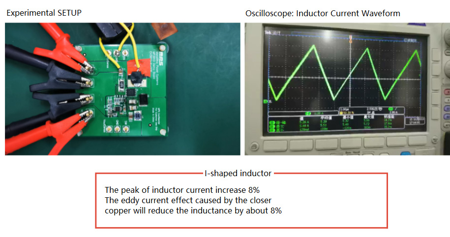
This experiment proves that laying copper on the bottom of the inductor has only a small effect on the inductance of the unshielded inductor, and has almost no effect on the inductance of the shielded inductor.
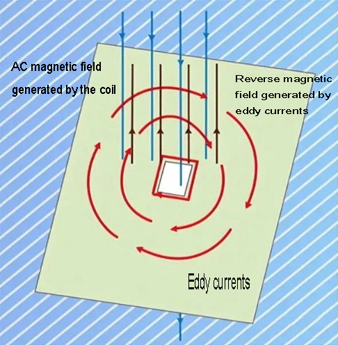
Before thinking about this problem, first review the understanding of the eddy current effect. The magnetic field line is from N to S level. When there is an alternating magnetic field passing through the surface of the conductor, it can be known from the law of electromagnetic induction that an induced current is formed on the surface of the conductor, and the direction of the magnetic field generated by the induced current will always play a role in weakening the size of the original magnetic field.
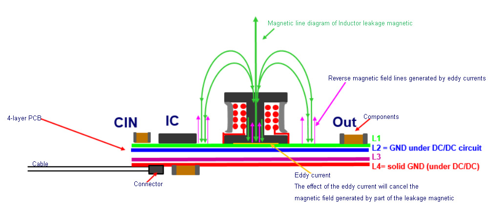
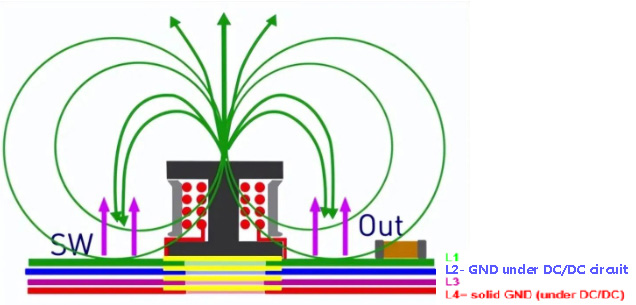
When the boost works normally, the load current flows through the inductor to form a loop. Due to the existence of the switch tube, the current changes dynamically, which can form the magnetic field line of the inductance. The magnetic field line on the surface of the conductor forms a closed magnetic circuit, and part of the magnetic circuit will form leakage flux and overflow into the air. If there is no copper coating on the bottom of the inductor, the magnetic field lines overflowing from the inductor will exist in the entire power supply system, so that the system has no relatively quiet space, which will cause the performance of EMI to decrease.
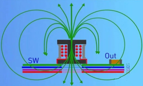
If the bottom of the inductor is laid with complete copper, the eddy current effect will be generated on the bottom plane of the inductor, and the eddy current will cancel the magnetic field generated by part of the leakage inductance, so that the original leakage magnetic induction line will be weakened. The bottom of the inductor is laid with copper, and the eddy current generated is like an electromagnetic shield, which blocks the downward propagation of the magnetic induction line, so that the high-frequency magnetic field generated by the inductor can be shielded on one side of the conductor, which greatly reduces the impact of the high-frequency magnetic field on other components in the space.
From two perspectives, from the perspective of EMI, it is recommended to laying copper; from the perspective of inductance, the shielded inductance has no effect, so copper is also recommended, and only the bottom of the I-shaped inductor is applied to the inductance, there is a little influence, so it depends on the situation in the actual project.
In the actual PCB layout, the filter at the switch is placed on the PCB plane opposite to the inductance, which is more conducive to avoiding high-frequency interference filter components and preventing high-frequency interference from being transmitted through the line.


