Table of Contents
Introduction
In the ever-evolving world of electronics, one component stands out as a fundamental building block: the Rigid Printed Circuit Board (PCB). These unassuming green or brown boards are the unsung heroes of our digital age, providing the foundation upon which our electronic devices are built. But what makes rigid PCBs so crucial, and why have they become an indispensable part of the electronics industry? This article delves into the world of rigid PCBs, exploring their technology, applications, manufacturing process, and the advantages they offer over other circuit board types.
What Exactly is a Rigid PCB?
At its core, a rigid PCB is a flat, inflexible board used to mechanically support and electrically connect electronic components. Unlike their flexible counterparts, rigid PCBs are designed to maintain their shape and structure, providing a stable platform for the intricate network of circuits and components that make up modern electronic devices.
Rigid PCBs are typically made from a variety of materials, with the most common being FR-4, a composite material composed of woven fiberglass cloth with an epoxy resin binder. This combination results in a board that is not only electrically insulating but also mechanically robust, able to withstand the rigors of manufacturing processes and daily use in electronic devices.
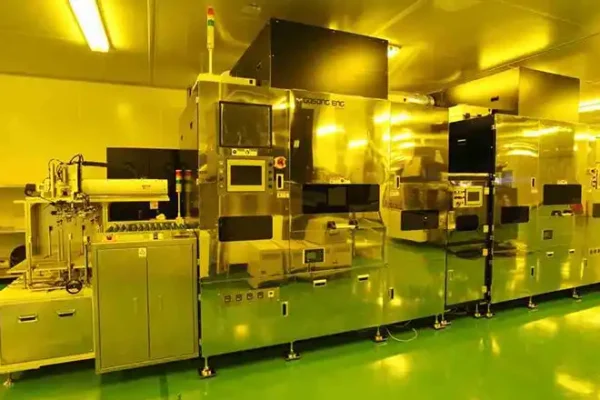
How Are Rigid PCBs Manufactured?
The manufacturing process of rigid PCBs is a complex and precise operation that involves several key steps. Understanding this process helps to appreciate the level of engineering and precision that goes into every board.
Material Preparation
The first step in rigid PCB manufacturing is the preparation of the base material. This typically involves cutting the FR-4 or other substrate material to the desired size and shape. The material is then cleaned thoroughly to remove any contaminants that could interfere with the subsequent processes.
Copper Cladding
Most rigid PCBs start with a layer of copper foil bonded to one or both sides of the substrate. This copper layer will eventually form the conductive pathways of the circuit.
Photoresist Application
A photosensitive film, known as photoresist, is applied to the copper-clad board. This film will be used to transfer the circuit pattern onto the copper.
Image Transfer
The circuit design is then transferred onto the photoresist using ultraviolet light. Areas exposed to the light harden, while unexposed areas remain soft and can be washed away.
Etching
The board is subjected to a chemical etching process that removes the unwanted copper, leaving behind only the desired circuit pattern.
Drilling
Holes are drilled into the board for component leads and vias (connections between layers in multi-layer boards).
Plating
For multi-layer boards, additional layers are added through a process of lamination and plating. This allows for more complex circuit designs in a compact space.
Solder Mask and Silkscreen
A solder mask is applied to protect the copper traces, and a silkscreen layer is added to provide component designators and other important information.
Final Inspection and Testing
The completed boards undergo rigorous inspection and electrical testing to ensure quality and functionality.
What Makes Rigid PCBs So Versatile?
One of the key strengths of rigid PCBs is their versatility. They can be designed in various configurations to suit different applications:
Single-Sided PCBs
The simplest form of rigid PCB, with components and circuits on one side of the board. These are cost-effective and suitable for basic electronic devices.
Double-Sided PCBs
These boards have circuitry on both sides, connected by vias. They offer more complexity and are widely used in consumer electronics.
Multi-Layer PCBs
Consisting of three or more conductive layers, these boards allow for highly complex circuit designs in a compact form factor. They are essential for advanced electronic devices like smartphones and computers.
What Are the Key Advantages of Rigid PCBs?
Rigid PCBs offer numerous advantages that have contributed to their widespread adoption in the electronics industry:
Durability and Reliability
The rigid structure of these PCBs provides excellent mechanical support for components, making them highly durable and reliable even in challenging environments.
Cost-Effectiveness
Thanks to well-established manufacturing processes, rigid PCBs can be produced cost-effectively, especially in large quantities.
Heat Dissipation
The solid structure of rigid PCBs allows for better heat dissipation compared to flexible alternatives, which is crucial for high-power applications.
Design Flexibility
Rigid PCBs can accommodate a wide range of component types and sizes, offering designers great flexibility in creating complex circuits.
Ease of Repair and Maintenance
The stable structure of rigid PCBs makes them easier to repair and maintain compared to flexible circuits.
Where Are Rigid PCBs Used?
The applications of rigid PCBs are virtually limitless, spanning across numerous industries and devices:
Consumer Electronics
From smartphones and laptops to televisions and gaming consoles, rigid PCBs form the backbone of most consumer electronic devices.
Automotive Industry
Modern vehicles rely heavily on electronics, with rigid PCBs found in everything from engine control units to infotainment systems.
Aerospace and Defense
Rigid PCBs are used in avionics, communication systems, and various military applications, where reliability is paramount.
Medical Devices
From diagnostic equipment to implantable devices, rigid PCBs play a crucial role in the medical field.
Industrial Equipment
Manufacturing machinery, process control systems, and robotics all depend on rigid PCBs for their operation.
What Challenges Do Rigid PCBs Face?
Despite their many advantages, rigid PCBs are not without challenges:
Space Constraints
As devices become smaller and more compact, fitting rigid PCBs into tight spaces can be challenging.
Weight Considerations
In applications where weight is a critical factor, such as aerospace, the relative heaviness of rigid PCBs can be a disadvantage.
Flexibility Limitations
Unlike flexible PCBs, rigid boards cannot be bent or folded to fit into uniquely shaped devices.
Environmental Concerns
The materials and processes used in rigid PCB manufacturing can have environmental impacts, prompting ongoing research into more sustainable alternatives.
What Does the Future Hold for Rigid PCBs?
As technology continues to advance, the future of rigid PCBs looks promising. Ongoing research and development are focused on several key areas:
Miniaturization
The push for smaller, more powerful devices is driving innovations in PCB design and manufacturing, allowing for even denser circuit layouts.
Advanced Materials
New substrate materials and conductive elements are being explored to enhance performance and reduce environmental impact.
3D Printing
Additive manufacturing techniques are being developed for PCB production, potentially revolutionizing the manufacturing process.
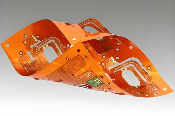
Integration with Flexible Technologies
Hybrid designs that combine rigid and flexible PCB technologies are becoming more common, offering the best of both worlds.
Conclusion
Rigid PCBs have earned their place as the backbone of modern electronics through their reliability, versatility, and cost-effectiveness. From the simplest consumer gadgets to the most advanced aerospace systems, these unassuming boards play a crucial role in powering our technological world. As we look to the future, rigid PCBs will continue to evolve, adapting to new challenges and enabling the next generation of electronic innovations. Their ability to provide a stable, durable platform for electronic components ensures that rigid PCBs will remain at the heart of our digital lives for years to come.

-600x400-c.png)