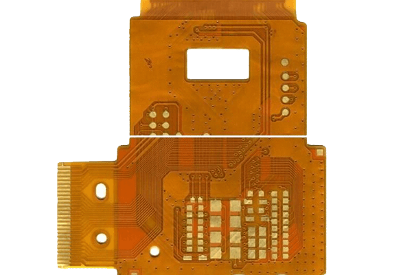
Via is an important part of multi-layer PCB board, drilling costs usually account for 30% to 40% of PCB board production costs. Therefore, through-hole design has become an important part of PCB design. In simple terms, each hole in a PCB board can be called a via.
From the view of role, vias can be divided into two categories: First, to be used as an electrical connection between the layers; Second, to be used as fixing or positioning points.
From view of process, vias are generally divided into three categories, blind hole (Blind Via), Buried hole (Buried Via) and through hole (Via).
The blind vias are located on the top and bottom surfaces of the PCB. They have certain depth to connect the surface line to the underlying inner wiring. The depth of the holes does not usually exceed a certain aspect ratio.
A buried hole is a connecting hole located on the inner layer of the PCB. It does not extend to the surface of the board. Using through-hole process and technology to form it, in its formation process may also overlap several inner layers.
The third type is through hole, which penetrates the entire circuit board, and can be used to achieve the internal interconnection or the component installation. As the through hole process is easier to achieve, cost is relatively lower than buried and blind hole, so majority of printed circuit boards are using it, rather than the other two type vias. From the design point of view, a through hole mainly consists of two parts, one is the drill hole, and the other is pad around the hole. The size of these two parts determines the size of the via.
Obviously, in the design of high-speed high-density PCB, the circuit board designers always want the smaller hole the better, so that PCB board surface can remain more layout space; the smaller the hole, its own parasitic capacitance is small, more suitable for high-speed circuits. However, the reduction in hole size results in increasing in cost, and the size of the vias can not be reduced indefinitely, as is limited by process technologies such as drill and plating. The smaller the hole, the longer time it takes to drill the hole, and the easier it is to deviate from the center.
Because of the limitations of technology or machinery, when the PCB thickness and hole size ratio (ie: aspect ratio) more than 10, Many PCB manufacturers can not guarantee the thickness uniformity of the hole wall copper, and copper layer thickness is uneven, especially the middle position of the hole, plated copper will become loose, too thin copper wall will seriously affect the fatigue life of the circuit board. Through years of experience accumulation and updates of machinery and equipment, Shenzhen PCB manufacturer – SysPCB thickness ratio already achieved 10: 1.


