Many people will face a problem when making high-frequency PCB: how to solve the power noise interference that appears on the high-frequency PCB board?
In this regard, a PCB technician said: we can destroy the occurrence conditions and effectively suppress the noise interference of the power supply. The specific solutions are as follows:
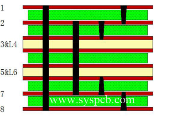
1) Pay attention to the through holes on the board
The through holes make it necessary to etch the openings on the power layer in order to leave space for the through holes to pass through. If the power layer is too open, it will inevitably affect the signal circuit, forcing the signal to bypass, the circuit area will increase, and the noise will increase. At the same time, if some signal wires are concentrated near the openng and share the circuit, the common impedance will cause crosstalk.
2) Place a power supply noise filter
It can effectively suppress the noise inside the power supply and improve the anti-interference and safety of the system. In addition, it is a two-way radio frequency filter, which can not only filter out the noise interference introduced by the power wire (to prevent interference from other devices), but also filter out the noise generated by itself (to avoid interference with other devices), and suppress the common-mode interference in serial mode.
3) Power isolation transformer
Separating the power loop or common mode ground loop of the signal cable can effectively isolate the common mode loop current generated by high frequency.
4) Power regulator
Regaining a cleaner power supply can greatly reduce power supply noise.
5) Wiring
The input and output lines of the power supply should not be arranged on the edge of the dielectric board, otherwise it is easy to generate radiation and interfere with other circuits or devices.
6) Separate the analog power supply and the digital power supply
High-frequency devices are usually very sensitive to digital noise, so they should be separated at the power inlet and connected together. If the signal crosses the analog and digital parts, a loop can be set at the intersection of the signal to reduce the loop area.
7) Avoid overlapping of independent power supplies between different layers
Stagger them as much as possible, otherwise power supply noise is easily coupled through parasitic capacitance.
8) Isolate sensitive components
Some components, such as phase-locked loops (PLL), are very sensitive to power supply noise. They should be as far away from the power supply as possible.
9) The connecting wire needs enough ground wire
Each signal needs to have its own dedicated signal loop, and the loop area of the signal and the loop should be as small as possible, that is, the signal and the loop should be parallel.
10) Place the power line
In order to reduce the signal loop, you can reduce noise by placing the power line close to the signal line.
In order to prevent the power supply noise interference on the circuit board and the accumulated noise caused by external interference on the power supply, the bypass capacitor can be grounded on the interference path (except for radiation) to bypass the noise to the ground and avoid interference with other equipment and device.
Conclusion
Power supply noise is directly or indirectly generated by the power supply and interferes with the circuit. When restraining its influence on the circuit, we must follow a general principle, that is, on one hand, we must try to prevent the influence of power supply noise on the circuit, and on the other hand, we should also minimize the influence of the external or circuit on the power supply to avoid deterioration of power supply noise.