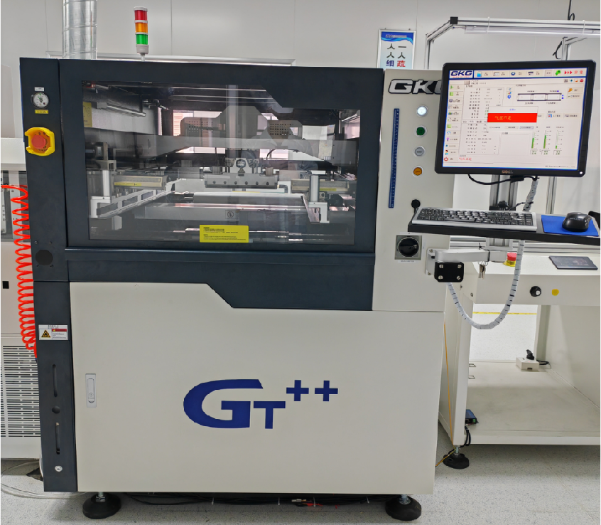
PCBA (Printed Circuit Board Assembly) testing fixtures are key tools used to test the functionality, performance, and soldering quality of PCBA. Their design and performance directly affect testing efficiency, accuracy, and production costs. The following are the main requirements for PCBA testing fixtures:
Table of Contents
1、 Electrical performance requirements
1. High precision contact
-The probe (such as Pogo Pin) needs to make precise contact with the PCBA test points (pads, vias, etc.) to ensure stable signal transmission and low contact resistance (usually<50m Ω), avoiding misjudgment caused by virtual soldering and poor contact.
-The probe spacing must strictly match the PCBA test point layout, with a tolerance controlled within ± 0.1mm, especially suitable for high-density circuit boards.
2. Signal integrity
-For high-frequency and high-speed signals (such as RF, USB, PCIe, etc.), fixtures should use low loss materials (such as polytetrafluoroethylene) and impedance matching design to reduce signal attenuation, crosstalk, and reflection.
-The grounding design should be reliable to avoid electromagnetic interference (EMI) affecting the test results.
3. Voltage resistance and insulation properties
-For high-voltage testing (such as insulation withstand voltage testing), fixtures must have high insulation performance (insulation resistance>100M Ω) to prevent leakage or breakdown and ensure testing safety.
2、 Mechanical structure requirements
1. Positioning accuracy and stability
-The fixture needs to be precisely aligned with the PCBA through positioning pins, card slots, and other structures to ensure that the probe is pressed vertically and avoid tilting or offsetting that may cause damage to the test point.
-Structural materials (such as aluminum alloy, electric wood, acrylic) need to be rigid, not easily deformed, and maintain accuracy under long-term use (usually with a service life of ≥ 100000 times).
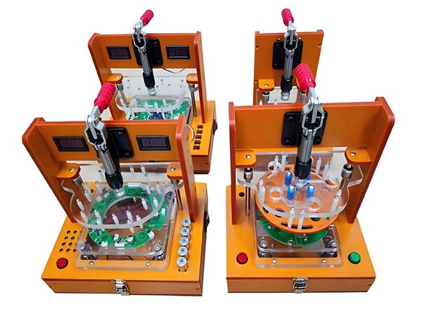
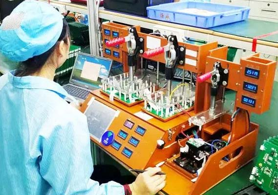
2. Convenience of operation
-Support fast clamping (such as pneumatic and manual pressing mechanisms), reduce loading and unloading time, and adapt to assembly line operations.
-Open design facilitates observation of the testing process, and faulty PCBA can be quickly removed for repair.
3. Compatibility and Scalability
-Compatible with multiple sizes and models of PCBA (by replacing the carrier board or probe module), reducing the cost of multi product changeover.
-Reserve expansion interfaces (such as sensors, pneumatic valves) for the integration of automated testing equipment (such as AOI, ICT, FCT).
3、 Reliability and durability requirements
1. Anti interference and anti-static
-Metal components need to be grounded to prevent static electricity from damaging sensitive components such as ICs and transistors; Non metallic materials should be made of anti-static materials (with a surface resistance of 10 ⁶ to 10 ⁹ Ω).
-Shielding design: For electromagnetic sensitive testing (such as sensor signals), a metal shielding cover needs to be added to reduce external interference.
2. Wear resistance and easy maintenance
-The probe should be made of high hardness material (such as beryllium copper gold plating) with a lifespan of ≥ 50000 times; Vulnerable components such as springs and sealing rings should be easy to replace.
-Modular design: The probe module and connecting wires can be independently disassembled for quick replacement in case of failure, reducing downtime.
4、 Security requirements
1. Anti misoperation and protection mechanism
-Protective barriers or insulation covers should be added to the live testing area to prevent operators from getting electrocuted.
-The emergency stop button and overload protection device (such as pressure sensors) should be sensitive and reliable to avoid damage to the PCBA caused by fixture abnormalities.
2. Compliance
-Compliant with safety standards such as UL and CE, materials must pass environmental certifications such as RoHS and REACH to avoid the use of harmful substances.
5、 Cost and efficiency optimization
1. Economy
-During mass production, the cost of fixtures needs to be controlled within a reasonable range (usually accounting for 10% to 30% of the total cost of testing equipment), balancing accuracy and cost.
-Standardized design: General components such as probe holders and guide rails can be reused, reducing customization costs.
2. Testing efficiency
-Support parallel testing of multiple workstations (such as testing multiple PCBAs at once), or linkage with automatic loading and unloading robots to improve production capacity.
-Integrate rapid detection modules (such as LED indicator lights and buzzers), provide real-time feedback on test results (Pass/Tail), and reduce manual interpretation time.
6、 Other special requirements
-Adaptability to high/low temperature environments: If testing is required at extreme temperatures, the fixture material should be temperature resistant (such as silicone or stainless steel) to avoid thermal expansion and contraction affecting accuracy.
-In high reliability fields such as medical/automotive electronics, fixtures must meet industry standards such as ISO 13485 and IATF 16949, and have traceability (such as numbering and calibration records).
-Customized interface: adapted to special testing requirements (such as flying pin testing for BGA chips, contact fixtures for flexible circuit boards (FPC)).
Summarize
The core goal of PCBA testing fixtures is to ensure accurate and efficient test results, while also considering usability, durability, and cost control. When designing, it is necessary to consider the characteristics of PCBA (such as component density, signal type), production scale, and industry standards, select appropriate fixture types (such as ICT fixtures, FCT fixtures, manual/pneumatic fixtures), and maintain performance stability through regular calibration (such as probe pressure testing, contact resistance measurement).
Ready to optimize your PCBA testing process? [Contact [SysPCB] for a fixture design consultation tailored to your specific throughput, reliability, and budgetary requirements.]