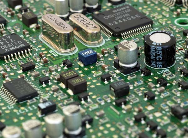
High speed PCB design is a crucial step in ensuring signal integrity, electromagnetic compatibility (EMC), and power stability. The following is a detailed explanation of its basic principles, combined with design specifications and engineering practice:
Table of Contents
1、 Functional zoning and signal flow optimization
1. Divide the area according to functional modules
Layout digital circuits, analog circuits, high-frequency circuits, power modules, etc. according to functional zones to avoid cross interference of different types of signals. For example, analog circuits and digital circuits need to be separated by isolation strips (such as ground plane separation) to prevent common mode noise coupling.
-Priority positioning of core components: With high-frequency/core components (such as CPUs and clock chips) as the center, related circuits are arranged around them to shorten the signal transmission path and reduce the loop area.

-Signal flow consistency: Ensure that the signal transmission direction is consistent (such as unidirectional flow from input to output), avoiding reflection and crosstalk.
2. Isolation of sensitive signals and interference sources
-High frequency signals:Such as clocks and high-speed differential lines, need to be kept away from high noise areas (such as power modules and I/O interfaces) and treated with grounding or shielding layers.
-Input/output isolation: The input circuit and output circuit should be placed separately to reduce the mutual influence of signal circuits.
2、 Layout rules for special components
1. High frequency components
-Shorten the connections between high-frequency components, reduce distributed parameters and electromagnetic interference (EMI), and keep input/output terminals as far away as possible.
-Adopting a symmetrical layout to avoid introducing phase differences due to asymmetric signal paths.
2. High voltage and power components
-Adequate spacing should be maintained between high-voltage components (such as a 2000V potential difference of ≥ 2mm) to avoid the risk of creepage.
-High power components (such as power modules) should be kept away from thermal sensitive components and heat dissipation should be enhanced through heat sinks or heat dissipation through holes.
3. Components that are susceptible to interference
-Sensitive components such as crystal oscillators and reset circuits should be kept away from high noise areas and isolated by shielding covers or ground planes.
3、 Principles of signal integrity design
1. Impedance control and matching
-Key signals (such as high-speed differential lines) need to maintain continuous characteristic impedance to avoid sudden impedance changes during interlayer switching.
-Differential lines follow the principle of equal length, with length deviation controlled within ± 5ml, and if necessary, compensated through serpentine routing.
2. Interference suppression
-The parallel line spacing meets the principle of 3W (line spacing ≥ 3 times the line width), and the differential line spacing meets the principle of 4W.
-The high-speed signal layer is vertically wired with adjacent planar layers to reduce interlayer crosstalk.
3. Topology optimization
-Adopting star topology or daisy chain topology in multi load scenarios to reduce signal reflection and timing deviation.
4、 Power and ground wire design
1. Power integrity
-Adopting a multi-layer board design, separate power layer and ground plane are set to reduce power impedance.
-The power input terminal is connected in parallel with a large capacitor (10 μ F~100 μ F) to filter out low-frequency noise, and a 0.1 μ F ceramic capacitor is added near the chip power pin for decoupling.
2. Ground level treatment
-Prioritize using the complete ground plane to avoid segmentation; If segmentation is required, connect through magnetic beads or 0 Ω resistors.
-Following the principle of 20H: the power layer shrinks relative to the formation by 20H (such as 40mil for a formation thickness of 2mm) to suppress edge radiation.
5、 Electromagnetic compatibility (EMC) measures
1. Shielding and filtering
-The high-frequency signal line adopts shielded wire and is grounded every 1000mil.
-Add TVS tubes or common mode inductors at the interface to suppress surges and common mode interference.
2. Reflection and radiation control
-Avoid placing critical signal lines (such as clocks) at the edges of the PCB to reduce edge effects.
-The high-speed signal routing avoids right angle turns and adopts 135 ° or circular arc transitions.
6、 Thermal Management and Mechanical Structure
1. Heat distribution optimization
-Reserve heat dissipation through holes around heating elements (such as power amplifiers) or enhance heat dissipation through copper foil laying.
-Keep a distance between high-temperature areas and sensitive components to avoid heat conduction affecting performance.
2. Mechanical strength and manufacturability
-Large components (weight>15g) need to be fixed with brackets to prevent displacement during welding.
-The PCB shape should preferably be rectangular (aspect ratio 3:2 or 4:3) to avoid stress concentration caused by irregular shapes.
7、 Design Verification and Simulation
-Combination of pre simulation and post simulation: Verify the integrity of key signals through electromagnetic field simulation (such as SIwave) during the layout phase, and check the timing margin through timing simulation (such as HyperLynx) after wiring.
-DRC rule check: Ensure that the safety spacing, number of via holes, and pad size meet the process requirements.
Summarize
High speed PCB design layout requires comprehensive electrical performance EMC、 Thermal management and manufacturability enable efficient and reliable circuit design through functional partitioning, impedance control, signal integrity optimization, and simulation verification. In practical applications, rules need to be flexibly adjusted according to specific scenarios. For example, high-frequency circuits emphasize impedance matching, while power supply design needs to focus on ripple suppression.
SysPCB is a well-known Chinese PCB manufacturer dedicated to providing high-quality PCB manufacturing solutions. We adopt advanced technology and strict quality control system to ensure that every PCB meets customer requirements.