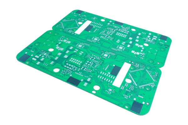
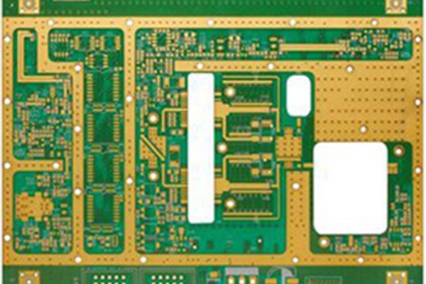
Ever since the printed circuit invented, building electronics has been made much simpler with the advent of the printed circuit board (PCB). They consist of a silicon board with multiple holes drilled for electronic components to be inserted. Electrical-Test is very important step in circuit board (PCB) manufacturing and assembly, it assure the function of PCB. Although your PCB already electrically tested by your PCB supplier, you might want test it by yourself.
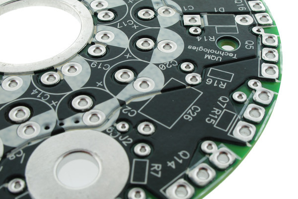
The holes are connected by varying patterns of copper lines that allow current to flow between the components. Typically when you are using a PCB you will solder each component to the desired hole. However, for the purpose of testing a printed circuit board, soldering will not be necessary.

Instructions
1. Wrap one of the wires around the positive terminal of the 9-volt battery. This is positive wire.
2. Wrap the other wire around the negative terminal of the 9-volt battery. This is the negative wire.
3. Study your PCB and find two sets of connected holes, or four holes total.
4. Connect the positive wire to one of the holes in the first set.
5. Connect the anode (long wire) of the LED to the second hole of the first set of holes on the PCB.
6. Connect the cathode (short wire) of the LED to the first hole of the second set of holes on the PCB.
7. Attach the negative wire from the 9-volt battery to the second hole of the second set of holes on the PCB.
8. Check to make sure the LED lights up. If the LED is illuminated, that particular section of the PCB is working correctly.
9. Follow this method on other sections of the PCB until you have tested all areas.
This testing can check for short circuits, open circuits and make sure the nets of the PCB boards that are identified as defective should be eliminated; defective PCB boards in panels should be specially marked.
Get your exclusive quote immediately: fill out the form or send an email directly.As a professional PCB manufacturer for hobbyist , we will provide you with a quote service within 24 hours. Enjoy free DFM optimization and a 10% discount on SMT patches for your first order!


