High layer circuit board is generally defined as 10 to 20 layers or more layers multilayer circuit board, process is difficult than the conventional multi-layer circuit boards, which require high quality and reliability. High layer PCB is mainly used in communications equipment, high-end servers, medical electronics, aviation, industrial, military and other fields. In recent years, demand from application communications, base stations, aviation, military and other fields remains strong, with the rapid development of China’s telecom equipment market, the high layer PCB is optimistic in market prospects.
At present, manufacturers capable of mass production of high layer PCBs, are mainly from foreign-funded enterprises and few domestic enterprises. High layer PCB production not only requires big technology and equipment investment, but also need technical and production staff to accumulate experience, while bring in high layer board customer need strict and cumbersome certification procedures, thus entering a high layer circuit board business is not easy for small PCB makers.
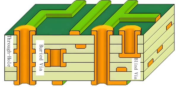
18 layer high layer pcb
The main producing difficulties of High layer PCB
Compared to conventional circuit board, high layer circuit board is thicker, more layers, more intensive lines and vias, larger outline size, thinner dielectric layer and other special characteristics, the alignment between inner layers, impedance control, and reliability requirements are more stringent.
1. Difficulties of alignment between the layers
Since many layers in high layer board, for better electronic performance, end clients increasingly require stringent alignment accuracy between inner layers, usual layer accuracy tolerance control is ± 75μm, consider high layer board is usually large size PCB; pattern transfer workshop temperature and humidity; the different cores sizing inconsistency causing dislocation overlay; targeting factors of aligning, the layer alignment between the high layer board is more difficult.
2. Difficulties in making the inner line
high layer board using special materials with high TG, high-speed, high-frequency, thick copper, thin dielectric layer and alike, demands high precision control on the inner line production and graphic size, such as the integrity of the impedance signal transmission, increasing the difficulty of making the inner line.
Because small line width/space, open/short increased, slightly short places increased. Because more fine line signal layer, the inner layer AOI missing chance increased. Inner layer thickness is thin, prone to fold and lead to bad exposure, core is too easy crack when etching; most of the high layer boards are large system board, big panel size, the cost is relatively high if there is scrap in process.
3. Lamination Difficulties
Multiple inner layer core and prepreg compress together, is prone to cause misalignment, delamination, resin voids and bubbles residues and other defects.
when design of the laminated structure, need to take full account of the material heat resistance, voltage, dielectric thickness and the amount of glue percentage in prepreg, and set a reasonable laminating program. Multi-layered, shrinkage control is more difficult, amount of compensation can not maintain consistency coefficient; insulating layer is thin, easily lead interlayer reliability test failures.
4. Drilling Production Difficulties
Using high TG, high-speed, high-frequency, thick copper laminates, will increase the roughness of mechanical holes, add difficult to de-burrs and etch drill fouling. Increase number of layers, will increase the cumulative total copper thickness and thickness, drilling bits is easy to break off, high dense BGA, narrow space between holes is prone to cause CAF failures, the board thickness increasing, easily lead oblique drilling problems.