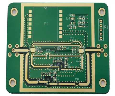
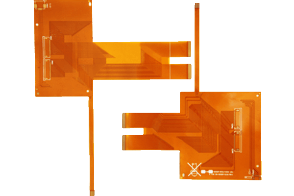
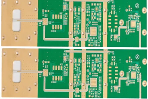
Generally, in my own experience of DIY circuit board, it can be divided into four processes:
1. Artwork — (by Protel or other relevant PCB layout software, then print the layout to a photo paper or film)
2. Exposing — (using table lamp or exposure light to transfer the image to photosensitive mask or film on circuit board)
3. Imaging— (using a etching solution, the exposed photosensitive film will be washed away, leaving the artwork of line and pads)
4. Etching — (wash away bare copper foil we don’t need, leaving copper foil covered by mask we need)
Here are 3 methods of DIY PCB, I prefer method2, the precision is good than other 2 methods.
Table of Contents
A: using pentel/masking tape
Using a pentel pen/masking tape mark your PCB with your circuit design/layout. Use the copper side when writing. Then submerge it in a basin using ferric chloride solution. Rock the basin back and forth to remove all the unwanted copper. Don’t let it soak too long! When the unwanted copper is removed you can now dry it. Letting it soak too long will also remove the copper in the pentel/masking tape. After letting it dry use a sandpaper and scratch the pentel pen marks of simply remove the masking tape. You can see clearly now that you’re circuit design has been etched into the PCB.

B: using a magazine/photo paper
You can also use a magazine or photo paper to etch a single sided PCB. You just have to print your circuit design in a glossy magazine or high quality photo paper. When printing, you should only use a laser printer. No other type of printers are allowed. After printing, iron the magazine/photo paper into the PCB until it sticks. Allow it to cool then remove it. Now you will submerge the PCB again into the basin full of ferric chloride. And repeat the same steps until you’ve etched the PCB with your layout.
C: using a photo resist pcb board
You can also try using a photo resist PCB board. This one you can buy at any electronic shops or even online shops like Amazon or Ebay. You only have to mark your PCB with your layout and put it under the sun and leave it for some hours. The copper will fade in time. You don’t have to soak it anymore in the ferric chloride. It’s easy but it will also cost you. Cheaper methods are listed above.


