Table of Contents
Any-Layer HDI PCBs: Unlocking Ultimate Miniaturization & Performance
Subtitle: Powering the Next Generation of Electronics with Advanced PCB Technology
Introduction
In the relentless pursuit of smaller, faster, and more powerful electronic devices, Printed Circuit Board (PCB) technology must continuously evolve. Any-Layer High-Density Interconnect represents the pinnacle of this evolution, enabling unprecedented levels of miniaturization and performance. As a leader in advanced PCB manufacturing, SysPCB leverages cutting-edge Any-Layer HDI capabilities to empower innovators across diverse industries. This article explores what Any-Layers HDI is, its critical applications, and the distinct advantages offered by SysPCB.
What is Any-Layer HDI?
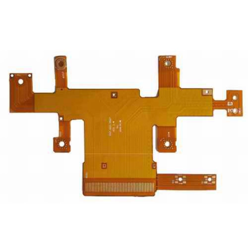
Any-Layer HDI is the most sophisticated form of HDI PCB technology. Unlike traditional HDI (which uses microvias typically only on outer layers or specific pre-defined layers) or standard PCBs, Any-Layer HDI allows for the placement of laser-drilled microvias (µvias) on any layer within the PCB stack-up.

•Core Technology: It utilizes sequential lamination processes, building the board layer-by-layer. Each layer can be individually laser-drilled to create microvias (usually ≤ 100µm in diameter) and interconnected as needed.
•Key Feature: Via-in-Pad: Microvias can be placed directly within component pads, maximizing routing density and freeing up surface area.
•Unparalleled Flexibility: Designers gain immense freedom to route complex, high-speed signals efficiently across all layers, overcoming the limitations of traditional via structures (like buried or blind vias confined to specific layer pairs).
•Ultra-Fine Features: Supports significantly finer trace widths/spacing (often down to 30-40µm or less), smaller capture pads, and higher connection pad density (pitch).
Why Any-Layer HDI Matters: The Driving Forces
* Extreme Miniaturization: Essential for shrinking device footprints (smartphones, wearables, IoT sensors).
* Enhanced Electrical Performance: Shorter signal paths and optimized routing reduce inductance, capacitance, and signal loss, crucial for high-speed digital (5G, AI processors) and high-frequency RF applications.
* Increased Functionality: Allows packing more features and components into a smaller space.
* Improved Thermal Management: Enables better heat dissipation pathways due to denser via placement.
* Superior Reliability: Microvias offer greater mechanical reliability than mechanically drilled through-holes, especially in demanding environments.
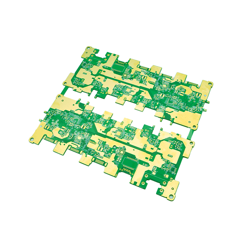
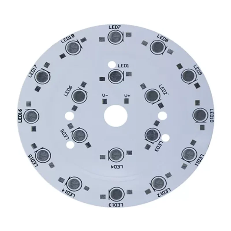
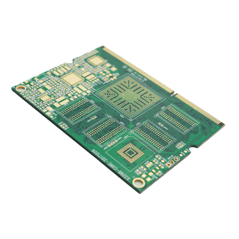
Key Applications of Any-Layer HDI Technology
Any-Layers HDI is indispensable for the most advanced and compact electronic devices:
1. Smartphones & Tablets: Core logic boards, camera modules, RF modules – enabling slim designs with powerful processors and multiple cameras.
2. Wearable Electronics: Smartwatches, fitness trackers, AR/VR headsets – where space is extremely limited.
3. High-Performance Computing (HPC) & AI: Server processors, GPUs, accelerators – managing immense data bandwidth and thermal loads.
4. Advanced Networking & Telecommunications: 5G base stations, routers, switches – handling ultra-high-speed data transmission.
5. Medical Electronics: Miniaturized implants, sophisticated diagnostic equipment, portable monitors.
6. Aerospace & Defense: Avionics, guidance systems, secure comms – requiring high reliability in harsh conditions and space-constrained platforms.
7. Automotive Electronics (ADAS, Infotainment): Advanced driver-assistance systems (ADAS), autonomous vehicle sensors, next-gen dashboards.
SysPCB: Your Trusted Partner for Any-Layer HDI Solutions
At SysPCB, we don’t just manufacture Any-Layers HDI PCBs; we master the complex engineering and precision manufacturing required for success. Here’s why leading global brands choose us:

1.Deep Expertise & Proven Process: Years of specialized experience in designing and fabricating complex Any-Layer HDI boards. Our robust process controls ensure consistency and reliability batch after batch.
2.Advanced Manufacturing Capabilities: State-of-the-art facilities equipped with precision laser drilling (CO2 & UV), advanced direct imaging (LDI), automated optical inspection (AOI/AXI), and stringent testing equipment.
3.Material Agnosticism & Expertise: Experience working with a wide range of high-performance laminates (low-loss, high-Tg, flexible materials) tailored to your specific electrical, thermal, and reliability requirements.
4.Design for Manufacturability (DFM) Support: Our engineering team collaborates closely with customers from the design phase, optimizing layouts for manufacturability, yield, performance, and cost-effectiveness.
5.Rigorous Quality Assurance: Comprehensive quality control adhering to IPC Class 2/3 standards and specific customer requirements. Advanced reliability testing (IST, thermal cycling) ensures product longevity.
6.Scalability & Global Support: Capable of supporting prototypes, NPI (New Product Introduction), and high-volume production runs. Dedicated customer support worldwide.
7.Commitment to Innovation: Continuous investment in R&D and process improvement to stay at the forefront of HDI technology.
Comparison Table: PCB Technologies at a Glance
| Feature | Conventional PCB | Standard HDI (1-n) | Any Layer HDI |
| Microvias | None / Limited | On outer/specific layers | On ANY Layer |
| Via-in-Pad | Difficult/Rare | Common (outer layers) | Common (All Layers) |
| Layer Count | Lower | Moderate to High | High to Very High |
| Line/Space | Larger (e.g., 100µm+) | Smaller (e.g., 75µm) | Finest (e.g., ≤40µm) |
| Routing Density | Lower | Higher | Highest |
| Miniaturization | Limited | Significant | Ultimate |
| Signal Integrity | Good | Better | Best (Short Paths) |
| Complexity/Cost | Low | Moderate to High | Highest |
| Typical Uses | Basic Electronics | Mobile Phones, Laptops | Smartphones, HPC, Wearables, Advanced Systems |
Conclusion
Any-Layer HDI is not just a PCB technology; it’s the enabling foundation for the next wave of electronic innovation. Its ability to deliver extreme miniaturization, superior electrical performance, and increased functionality makes it critical for cutting-edge applications across diverse sectors.
SysPCB possesses the specialized expertise, advanced manufacturing capabilities, and unwavering commitment to quality required to successfully bring your most demanding Any Layer HDI designs to life. We partner with you to overcome complexity and achieve optimal performance, reliability, and time-to-market.
Ready to push the boundaries of your next electronic product?
Contact the Any Layer HDI experts at SysPCB today for a consultation!