Availability: | |
---|---|
In the periodic table of chemical elements, the elements of group ⅦA of the periodic system refer to halogen elements, including fluorine (F), chlorine (Cl), bromine (Br), iodine (I), and astatine (At).
According to the JPCA-ES-01-2003 standard, copper clad laminates with chlorine (Cl) and bromine (Br) elements less than 0.09% Wt (weight ratio) are defined as halogen-free copper clad laminates. (JPCA is the abbreviation of Japan Electronic Circuit Industries Association.)
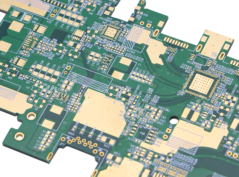
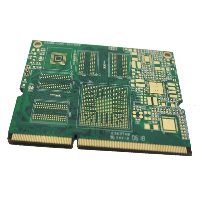
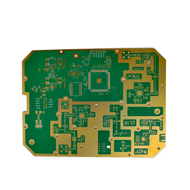
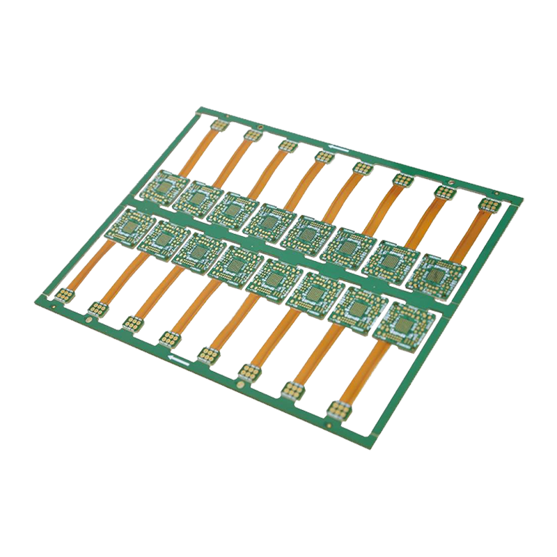
Halogen free PCB refers to printed circuit boards with halogen content that meets specific limit standards. The International Electrotechnical Commission (IEC) defines halogen-free PCB as a circuit board with a total halogen content not exceeding a certain limit.
Halogen free PCBs mainly achieve their environmental characteristics by using flame-retardant materials that do not contain halogens. These materials do not release toxic gases such as dioxins when burned, thereby reducing their harm to the environment and human health.
The mainstream resin composition of halogen-free PCBs usually includes phosphorus containing epoxy resin and phenolic resin. Phosphorus containing epoxy resin can improve heat resistance, flame retardancy, and dielectric properties, while phenolic resin can enhance the heat resistance and adhesion of materials.
In the manufacturing process, new raw materials such as modified polymer resins and surface treated inorganic fillers are widely used. These materials can enhance the flexibility, adhesion, and flame retardancy of the board.
The manufacturing process of halogen-free PCBs is relatively complex and requires the use of specific drilling parameters and equipment. Due to the increased rigidity and high thermal decomposition temperature of halogen-free materials, the drilling parameters of ordinary FR-4 may not be applicable and need to be adjusted appropriately under normal conditions.
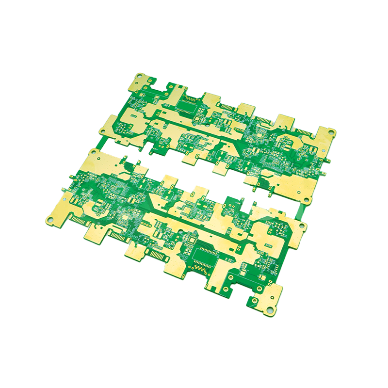
Advantages of halogen-free PCB
Halogen free PCBs reduce the use of halogen containing chemicals in the production process and lower the pollution level of wastewater and exhaust gas. It does not release toxic gases during combustion, reducing environmental pollution and harm to human health.
Halogen free PCBs exhibit excellent performance in electrical insulation, thermal stability, and water absorption. Its insulation resistance and resistance to breakdown are stronger, its coefficient of thermal expansion is smaller, and its water absorption is lower.
Things often have two sides. The advantages of halogen-free boards are at the cost of increasing complexity, not only in the PCB manufacturing process but also in the PCB design. There are differences between halogen-free PCB and conventional PCB, such as drilling.
The P and N series functional groups used in the halogen-free board increase the molecular weight and enhance the rigidity of the molecular bond, resulting in increased rigidity of the material. At the same time, the TG point of the halogen-free material is generally higher, so the effect of using the ordinary FR-4 drilling parameters to drill is not satisfactory. When drilling halogen-free boards, some adjustments should be made under normal drilling conditions.
(1) It has been found that its typical resin formula can contribute to further performance improvements, such as enhancing the heat resistance of the board; The reduction of the tangent of the dielectric loss angle is something that traditional FR-4 CCL cannot achieve.
(2) Similar to the lead-free compatibility FR-4, its performance weaknesses (such as micro hole processability and heat resistance after moisture absorption) are exposed, and improvements are needed in this area of performance.
Halogen free PCB boards have a wide range of applications, including but not limited to network communication equipment, automotive electronics, industrial control, medical equipment, and other fields. The manufacturing technology of this type of board is constantly evolving to meet the needs of different applications.
For example, by changing the resin system and using non bromine based resins to achieve environmentally friendly substrates, the most widely used one is epoxy resin. When in liquid state, it is called A-Stage or Varnish. When immersed in reinforcing materials such as glass cloth and quickly dried, it is called B-Stage, which is a semi cured sheet. After being cured by a high-temperature pressing plate, it becomes a cured board of C-Stage.
At present, the flame retardant CCL substrates FR4, CEM-1, CEM-3, etc. used in the circuit board market are mostly brominated epoxy resins.
Relevant institutions have done research on epoxy resin substrates: when halogen-containing flame-retardant substrates are discarded and burned, they will release harmful substances such as dioxins. This substance has an unpleasant smell, is highly toxic, and can cause cancer. Once inhaled, it cannot be discharged, which will cause huge harm to the human body.
The halogen-free board realizes the environmental protection and non-toxicity of the PCB by replacing or reducing these harmful elements.
Halogen containing substrate: a flame retardant mixture composed of halogenated polymers or halogenated flame retardants, commonly including brominated flame retardants such as decabromodiphenyl ether and antimony trioxide.
Halogen free substrate: Use halogen-free organic flame retardants, such as phosphorus nitrogen organic flame retardants, such as triazine ketone compounds and triazine triamine compounds.
Halogen based materials: When burned, they produce a large amount of smoke and toxic corrosive hydrogen halide gas, posing a threat to the environment and human health.
Halogen free substrate: produces less smoke during combustion, does not produce toxic gases, and is more environmentally friendly.
Halogen based materials: Low cost, but limited in scope due to poor environmental performance, mainly used in occasions with low environmental requirements, such as ordinary electronic devices and home appliances.
At present, most of the halogen-free materials are mainly phosphorus-based and phosphorus-nitrogen-based. What's interesting is that high polymer resins containing phosphorus and nitrogen compounds will produce non-combustible gas when burned. This gas can isolate the burning surface of the resin from the air and achieve the purpose of flame retarding.
Material selection: Halogen free materials are more difficult to obtain compared to traditional halogen materials, and selecting suitable halogen-free materials has become the primary issue in the manufacturing process.
Inter layer signal interference: In multi-layer PCB circuit boards, the stacking of signal and power layers can easily cause inter layer signal interference, which requires the use of inter layer isolation technology and appropriate inter layer grounding solutions to solve this problem.
Mismatch in thermal expansion coefficient: The thermal expansion coefficients of halogen-free materials and halogen materials are different, which can easily lead to material splicing problems during temperature changes, requiring special material matching and process control.
Blacking and carbonization: Halogen free materials are prone to blackening or carbonization during high-temperature sintering, which affects circuit performance. Therefore, strict control of sintering temperature and time is required during the manufacturing process.
Poor processing performance: Halogen free materials usually have high hardness and brittleness, and are prone to breakage during processing. Suitable process parameters and processing methods need to be adopted to solve this problem.
Electroplating protection performance: Coating adhesive on the surface of halogen-free materials can protect the surface of circuit boards, but it will have a certain impact on the electroplating process, and the coating and degreasing processes need to be optimized.
Cost issue: The materials and manufacturing process of halogen-free multilayer PCB boards are more complex and expensive than traditional halogen materials, and the manufacturing cost is relatively high.
We prioritize our customers, offering exceptional support and prompt responses to inquiries at any time. Here’s why SysPCB is the ideal choice for your halogen-free PCB needs:
Extensive Expertise: Over a decade of experience in halogen-free PCB manufacturing.
Affordable Solutions: Competitive pricing with no minimum order quantity (MOQ) and flexible, negotiable terms.
Superior Quality: High-quality assurance backed by professional production facilities.
Comprehensive Services: End-to-end solutions with a strong focus on customer satisfaction throughout the process.
Timely Delivery: Fast turnaround times paired with reliable post-sales support.
Key layout principles include ensuring an even distribution of components, maintaining consistent arrangement angles, and providing adequate spacing around large components like BGAs and QFPs. Heat-radiating components should be placed in ventilated positions away from sensitive parts, while frequently adjusted components must be easily accessible. Proper spacing must account for thermal expansion, stress sensitivity, and large component tolerances. Additionally, PCB designs exceeding 500cm² should incorporate support structures to prevent bending during reflow soldering. Component placement should align with the reflow oven's conveyor belt angle to ensure thermal symmetry and optimal heat capacity. Adhering to spacing requirements ensures manufacturability, testability, and maintainability in SMT assembly.
The KB6160 is a high-performance integrated circuit designed for applications in consumer electronics, industrial automation, automotive systems, and IoT devices. This blog explores its key specifications, including a 3.0V to 5.5V operating voltage range, -40°C to +85°C temperature range, and up to 50 MHz clock speed. The IC features low power consumption, high-precision ADC/DAC capabilities, multiple GPIO ports, and embedded protection. Typical applications include smartphones, industrial sensors, automotive ECUs, and IoT solutions. Design considerations such as thermal management and signal integrity are discussed. For complete technical details, the official KB6160 datasheet provides comprehensive guidance.
The KB6165 is a high-performance integrated circuit designed for diverse applications in consumer electronics, industrial automation, automotive systems, and IoT devices. This blog highlights its key specifications, including an operating voltage range of 3.0V to 5.5V, operating temperature range of -40°C to +85°C, and clock speeds up to 50 MHz. The IC features low power consumption, high precision ADC/DAC capabilities, multiple GPIO ports, and embedded protection. Typical use cases range from smartphones to industrial sensors and automotive ECUs. Guidance on design considerations, such as thermal management and signal integrity, is provided to ensure optimal performance. For detailed implementation, refer to the official KB6165 datasheet.
Linear regulators are available in fixed, adjustable, and programmable output versions. Fixed output regulators provide a specified voltage range rather than an absolute voltage, influenced by factors like load current, temperature drift, and reference voltage stability. The deviation from the rated voltage is due to the non-ideal characteristics of components such as Zener diodes and internal resistance.
Semiconductor optoelectronic devices enable the reversible conversion between light and electrical energy, utilizing specialized materials and processes for diverse applications. These components collectively represent the core technologies driving advancements in electronic systems.
Many projects of hardware engineers are completed on perforated boards, but there is a phenomenon that the positive and negative poles of the power supply are accidentally reversed, causing many electronic components to be burned, and even the entire board is scrapped, and another piece has to be so