For each new electronic product, after the designer comes up with a design concept, the electronic engineer will start the circuit design and circuit layout, and then first make a prototype Printed Circuit Board (PCB) to verify whether the design concept is feasible, and then conduct a small batch trial production, and finally can be mass-produced and marketed. Prototype PCB fabrication is an essential step in these steps.
SysPCB, as a professional PCB manufacturer in China, Now let’s give a comprehensive introduction to the prototype Printed Circuit Board (PCB).
Table of Contents
What is a prototype PCB?
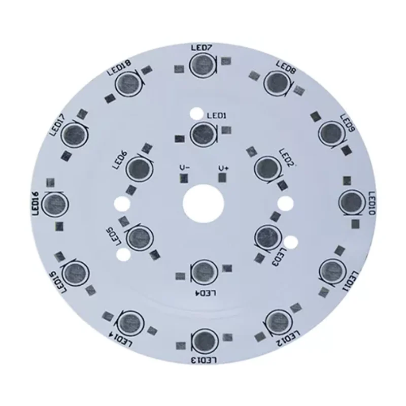
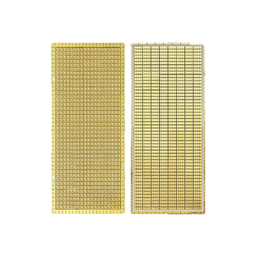
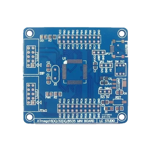
Prototype PCB refers to trial production before mass production of the PCB, which is essentially an early sample of the product. In the process of prototype PCB production, engineers often design different circuit boards and manufacturing specifications for testing in order to select more suitable products (including appearance, cost, function, and other considerations). There is generally no specific limit to the production quantity of PCB prototypes. Usually, engineers refer to a product design as a PCB prototype before confirming it.Prototype PCB
The benefits of prototype PCB
1. Shorten time and save costs
Engineers may go through several design iterations before creating the final product. And with products on the market changing all the time, time is a very important factor in this industry. You need to be able to test new designs quickly in order to complete production in a timely manner, as a lengthy design process can lead to excessive losses. But prototype PCB can help speed up the entire design and manufacturing process by following methods:
1) Complete testing
Prototype PCB can help PCB design engineers test design problems quickly and accurately. Without this one point, finding design flaws takes more time, and if not delivered on time, it can lead to customer dissatisfaction, which can result in a loss of revenue.
2) Customers see the product in advance for better communication
Customers often want to see the product at multiple points in the production process, and providing prototypes as an aid can help to better communicate the design concepts, as well as communicate most effectively with the customer.

3). Minimize rework and help batch manufacturing go smoother
PCB testing allows you to view and test boards before they go into production, reducing rework in small pilot or volume production. The earlier you find design flaws in your PCB design, the less expensive it will be to fix them. If you don’t use prototype PCB boards to test your design and put a defective product into production, you may run into problems later in the production run that cost more and will take longer.
2. Test and view product features in advance
Having an accurate and reliable prototype Printed Circuit Board (PCB) makes it easier to solve design problems throughout the development process. High-quality prototype preparation represents the functionality of the final product and can help engineers view and test the following areas:
PCB Design
Prototyping helps engineers to identify defects as early as possible in the development process. The more accurate the design, the more accurate the defect identification, which can minimize design costs and also reduce project time.
Functional testing
There are some things that are theoretically effective, but in practice they are not. An accurate prototype Printed Circuit Board (PCB) can check and evaluate some of the features of the product and helps in evaluating the theoretical values and you can see if they appear in the actual values.
Condition testing
Many products are required to be applied to special environments, so PCB products must be properly tested to be able to ensure proper operation in the environment. So, using prototype PCBs can be carry out temperature change tests, power change tests, shock resistance tests and so on.
3. Separate test components
Engineers often create prototype PCBs for testing, and one of the most useful tests is testing individual components and functions. The ability of a PCB board to work depends on the integration of all components on the board. Testing a single component helps engineers to test individual functions efficiently. It can ensure that each component can function as expected, and also find invalid components for timely replacement with valid ones.
4. Improve the final product
Prototype PCB design helps to improve the PCB and each component, thereby achieving higher quality design.
In some cases, adjustments to the PCB will result in a slightly different PCB shape or material than originally planned, which may affect the overall product specifications and manufacturing requirements.
Prototype PCB can determine whether it is necessary to adjust the product as soon as possible, then improve, plan, and reduce the product and its related costs.

PCB prototype concerns:
⑴ PCB manufacturing Speed
Products in the PCB market change all the time. In this industry, time is a very important factor. Delivery time is the competitiveness of PCB factories, and SysPCB is one of the most favored factories for engineers, because now we provide expedited service, with the fastest delivery time of 24 hours.
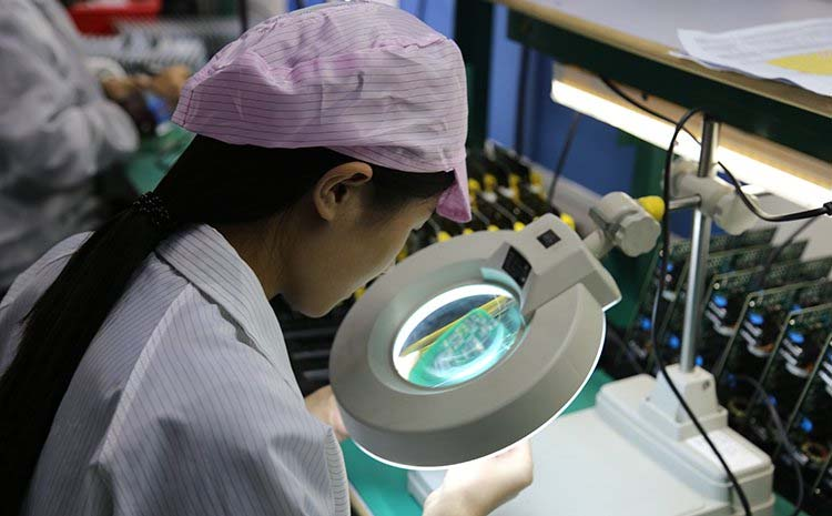
⑵ PCB prototype Quality
It is a trial production by engineers before the product design is confirmed and tested, and the quality cannot be ignored. From raw materials, schematic drawing, to production, testing, quality control, etc., every link needs to be strictly checked. For example, for ordinary double-sided boards, the raw materials generally include FR-4, aluminum substrate, CEM-1, etc., the thickness of the board is from 0.4mm to 3.0m, etc., and the thickness of copper is 0.5oz to 3.0oz. The difference of these materials causes the difference between quotations very large. At present, the better materials used by manufacturers are Shengyi, Isola CCL.
⑶ PCB prototype Price
With the development of the industry, the price of PCB prototype, small and medium batch PCB production is constantly falling. Use challenging prices to complete challenging tasks, which will be the price trend of the future circuit board prototype.
Preparations for PCB Prototype
1. Physical border production
The physical frame is a basic platform for future component layout and PCB prototype. Be sure to pay attention to accuracy. Furthermore, it is best to use arcs in the corners, which can not only avoid PCB being scratched by sharp corners, but also reduce stress.
2. Introduce components and networks, and lay out components
When introducing components and networks into the drawn frame during PCB prototype, you must carefully follow the prompts, including the packaging form of components and component network problems. Because of the comparison tips, it is not easy to have problems. The layout of components and traces during PCB prototype has a great impact on the product’s life, stability, and electromagnetic compatibility, and should be paid special attention to. Generally speaking, there should be the following principles: placement order, pay attention to heat dissipation.


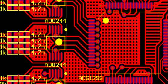
3. PCB design and wiring and adjust and improve
It is best to pay attention to the requirements of processing parameters during PCB design and wiring, or discuss with a reliable PCB prototype manufacturer, the defective rate will be greatly reduced. After completing the PCB design and wiring, all you need to do is to make some adjustments to the text, individual components, and traces and apply copper plane (this work should not be done too early, otherwise it will affect the speed and bring trouble to the PCB design and wiring), also it is convenient for production, debugging and maintenance.
4. Check the network
Sometimes the network relationship of the drawn PCB board is different from the schematic diagram due to misoperation or negligence. At this time, it is necessary to check. Therefore, after drawing, you should check it first, and then carry out follow-up work.
The above are some introductions related to the prototype PCB, hoping to be helpful to you. If you want to learn more about PCB prototype information, please feel free to contact us at any time.
Why Choose SysPCB as Your PCB Prototyping Service Provider?
Here’s why choosing us is the best decision for your prototype PCB needs:
Fast Turnaround Time
As a leading prototype PCB supplier in China, we pride ourselves on delivering high-quality prototype PCBs with rapid turnaround times. With our state-of-the-art fabrication and testing equipment, we ensure that your prototypes are ready quickly, enabling you to bring your products to market sooner and accelerate your return on investment. We work closely with clients to accommodate any design changes or iterations during the fabrication process.
High-Quality Prototype PCB
We are committed to manufacturing only the highest-quality PCBs that meet all industry standards and customer specifications. As trusted PCB prototype manufacturers, we follow established procedures to ensure top-notch performance and reliability. Our continuous improvement approach ensures that we consistently provide better service and quality with every project.
No MOQ
SysPCB does not have a minimum order quantity (MOQ) requirement, so you can confidently partner with us. As an China PCB manufacturer, we are committed to building long-term relationships based on mutual trust and benefit.
As reliable China PCB manufacturers, SysPCB is committed to delivering the best prototype services, tailored to meet your unique needs. Contact us today to get started!
Hot tags: China PCB, express pcb, fabricate pcb, circuit board services, ordering pcb, circuit board prototype, prototyping board, proto board, prototype board, breadboard, Customized, cheap, quotation, suppliers, factory, manufacturer, manufacturing, manufacturing services