Table of Contents
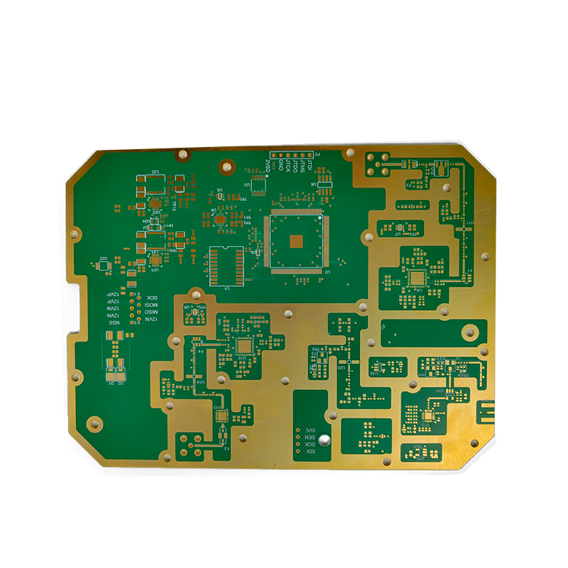
What is Bare PCB?
Bare PCB is a type of circuit board that has not undergone circuit board control processing and printed circuit patterns. It does not include any circuit components during the manufacturing process. This type of circuit board typically has conductive tracks and sufficient pad space, allowing users to freely design circuit layouts and assemble circuit components.
Types of Bare PCB(bare circuit boards)
Generally, bare circuit boards can be divided into three types: single panel, double-sided board, and multi-layer board.
1. Single PCB
Single panel refers to a circuit board with only one side covered with copper and only one side chemically etched. Single panel is usually only suitable for simple circuits, so the manufacturing cost is relatively low.
2. Double sided PCB
Double sided board refers to a circuit board with connected circuits on both sides that do not affect each other. Double sided panels are more suitable for complex circuits than single panel panels, but the manufacturing cost is also higher.
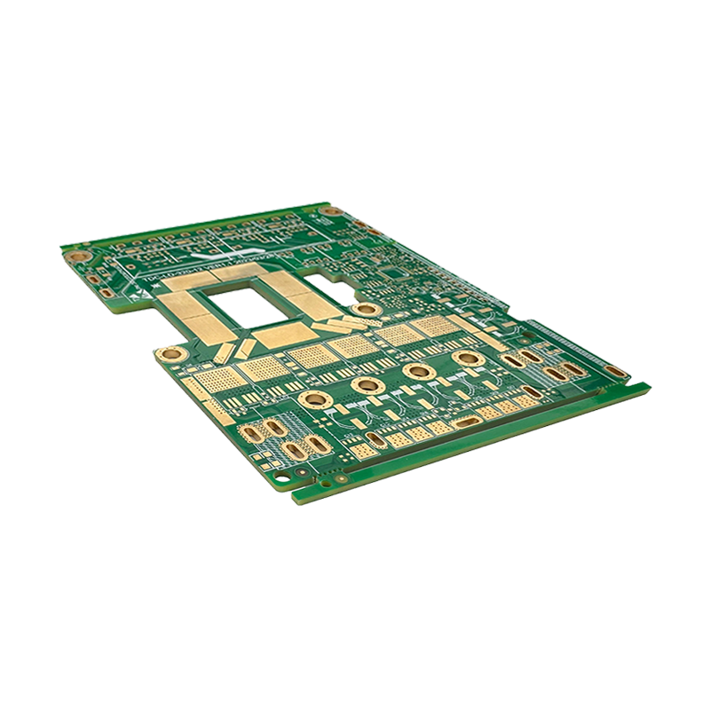
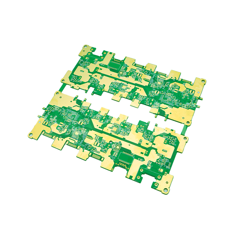
3. Multilayer PCB
Multilayer board refers to the process of laminating multiple single or double-sided boards, typically consisting of four or more layers. Multilayer boards not only have more complex circuits, but can also achieve smaller volumes, but they are also more expensive compared to double-sided boards and single panel boards.

Production and manufacturing process of Bare PCB(bare circuit boards)
(1) Preliminary preparation
The preliminary preparation includes checking the raw materials (FR-4 or metal substrate), designing the network cable diagram of the circuit board, designing circuit board software, and mastering drawing skills.
(2) Produce inner layer board
By cutting and stacking copper foil, an inner layer circuit board is obtained with a board thickness of 0.035-0.070mm.
(3) Pattern exposure
Copy the silk screen network diagram onto the inner board, or export it using methods such as shielding film coating or etching.
(4) Etching
Etch the circuit board in a controlled environment to remove unwanted metals and obtain the basic shape.
(5) Outer panel production
Perform double-sided bonding, pressing, processing, and other operations on the processed inner panel.
(6) Surface coverage
Cover the outer board with anti-corrosion and printing layers through spraying, printing, immersion plating, and other methods. The anti-corrosion coating is usually composed of welding film, shielding electrostatic film, semi-solid coating film or OSP film, etc.
(7) High temperature drying
Arrange a well ventilated and clean drying room in the factory for high-temperature drying to densify the epoxy resin between the layers of the circuit board.
(8) Final performance check
Inspect the circuit board by powering it on to ensure that it is functioning properly.

Bare PCB plays an important role in electronic product manufacturing:
- Testing platform: used for testing and debugging in the development process of electronic products to avoid problems after manufacturing.
- Product validation: Provide a reliable validation platform to confirm the effectiveness and performance of circuits, identify and resolve design errors.
- Cost reduction: With low production costs, it can greatly reduce the manufacturing cost of electronic products, improve product production efficiency and quality.
Differences from other related concepts:
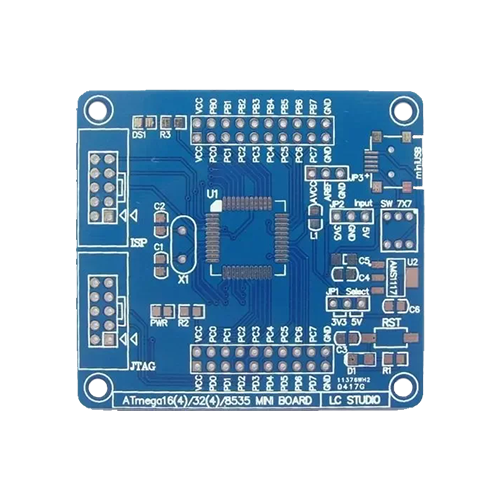
The difference between Bare PCB and PCBA lies in whether electronic components are assembled. PCBA is a circuit board that has already been assembled with components, while an empty circuit board is unassembled.
SysPCB: Your Trusted Partner in Fabricating Bare PCBs
SysPCB‘s bare PCB product line allows you to have a smooth and effective development experience:
Extensive Experience
Backed by over 10 years of expertise in bare PCB manufacturing.
Superior Quality Standards
Our bare PCBs are produced to the highest standards through our network of reliable and trusted suppliers.
Advanced Manufacturing Techniques
We offer cutting-edge fabrication options, including plated slots, impedance control, blind and buried vias, and micro-drilled vias to meet your design needs.
On-Time Delivery
Dependable turnaround times combined with robust post-sales support.