

Table of Contents
1、 Collaborative evolution of communication equipment and PCB board
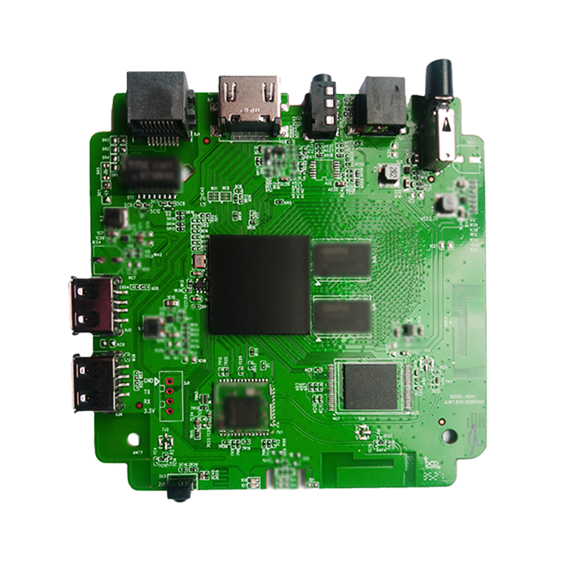
In modern communication infrastructure such as 5G base stations, optical transmission equipment, and satellite communication systems, PCB circuit boards play a critical role similar to neural networks. As a professional communication PCB manufacturer in China, we have been deeply involved in this technological evolution process as a communication PCB manufacturer. Our research and development data shows that the PCB integration density of the new generation of communication equipment has increased by 300% compared to the 4G era, and the signal transmission rate has exceeded 112Gbps. These breakthroughs directly promote the global leading speed of 5G base station construction in China.
2、 Classification and technological innovation of communication grade PCB boards
2.1 High reliability rigid PCB
Using FR-4 and Rogers RO4000 series high-frequency laminates, impedance control is achieved through 8-32 layer precision stacking design. As a communication PCB manufacturer, we have introduced German laser direct imaging equipment to achieve ± 25 μ m line accuracy and ensure the integrity of 5G millimeter wave frequency band signals.
2.2 Form Revolution of Flexible PCB
By using polyimide substrate combined with copper rolling process, the bending radius can reach 0.5mm. Our customized 3D folding screen PCB solution for a leading mobile phone manufacturer has successfully passed 200000 dynamic bending tests, helping them achieve a breakthrough in terminal product form.
2.3 System integration of rigid flexible composite panels
By using laser drilling and stepped pressing technology, the rigid zone and flexible zone are seamlessly connected. The radar array module developed by us as a communication PCB manufacturer adopts a 12 layer rigid flexible board design, which reduces equipment volume by 40% and increases installation flexibility by 60%.

3、 Innovative Application Cases in the 5G Era
3.1 Large scale MIMO antenna array
Adopting a mixed pressure structure PCB, Rogers RO4835 is used in the high frequency band, and FR-4 material is used in the low frequency band. Our 64T64R antenna board achieves ± 0.75dB amplitude consistency, helping customers increase their base station coverage radius by 35%.
3.2 High speed Interconnection Scheme for Optical Modules
A 20 layer backplane based on Megtron 6 material has an eye diagram margin of 25% at a rate of 112Gbps. We provided CPO co packaged PCBs for a data center, reducing the interconnect loss from the optical engine to ASIC to 0.8dB.
4、 As a communication PCB manufacturer, we are the benchmark for intelligent manufacturing of communication PCBs in China
As a national high-tech enterprise, we have built a 150000 square meter intelligent production base equipped with fully automatic electroplating lines and AOI intelligent detection systems. Through 18 professional certifications such as IATF16949/ISO13485, our products have been exported to 23 countries and regions, and we have obtained a total of 56 invention patents.

5、 PCB technology reserves for 6G
We are developing D-band PCB samples based on liquid crystal polymer (LCP), with dielectric loss controlled below 0.002. The three-dimensional heterogeneous integration technology realizes the integrated packaging of chip antenna PCB, providing basic support for terahertz communication.
conclusion
In the wave of intergenerational changes in communication technology, as a communication PCB manufacturer, we have always adhered to material innovation driven process breakthroughs. From the current industry position of 23% market share in 5G base station PCBs to the ongoing construction of 6G R&D centers, we continue to provide high value-added PCB solutions for global communication equipment manufacturers, fulfilling our corporate mission of “connecting the world and transmitting the future”.